Dc electrical characteristics – Rainbow Electronics DS92LV010A User Manual
Page 3
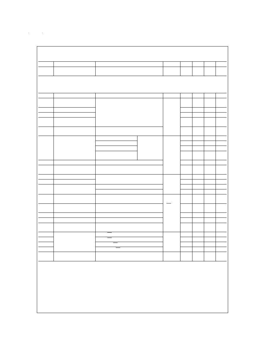
DC Electrical Characteristics
(Notes 2, 3) (Continued)
T
A
= −40˚C to +85˚C unless otherwise noted, V
CC
= 3.3V
±
0.3V
Symbol
Parameter
Conditions
Pin
Min
Typ
Max
Units
C
output
Capacitance
@
BUS
Pins
DO+/RI+,
DO−/RI−
5
pF
DC Electrical Characteristics
(Notes 2, 3)
T
A
= −40˚C to +85˚C unless otherwise noted, V
CC
= 5.0V
±
0.5V
Symbol
Parameter
Conditions
Pin
Min
Typ
Max
Units
V
OD
Output Differential
Voltage
R
L
= 27
Ω
,
Figure 1
DO+/RI+,
DO−/RI−
145
270
390
mV
∆
V
OD
V
OD
Magnitude Change
3
30
mV
V
OS
Offset Voltage
1
1.35
1.65
V
∆
V
OS
Offset Magnitude
Change
5
50
mV
I
OSD
Output Short Circuit
Current
V
O
= 0V, DE = V
CC
−12
−20
mA
V
OH
Voltage Output High
V
ID
= +100 mV
I
OH
= −400 µA
R
OUT
4.3
5.0
V
Inputs Open
4.3
5.0
V
Inputs Shorted
4.3
5.0
V
Inputs
Terminated, R
L
= 27
Ω
4.3
5.0
V
V
OL
Voltage Output Low
I
OL
= 2.0 mA, V
ID
= −100 mV
0.1
0.4
V
I
OS
Output Short Circuit
Current
V
OUT
= 0V, V
ID
= +100 mV
−35
−90
−130
mA
V
TH
Input Threshold High
DE = 0V
DO+/RI+,
DO−/RI−
+100
mV
V
TL
Input Threshold Low
−100
mV
I
IN
Input Current
DE = 0V, V
IN
= +2.4V, or 0V
−20
±
1
+20
µA
V
CC
= 0V, V
IN
= +2.4V, or 0V
−20
±
1
+20
µA
V
IH
Minimum Input High
Voltage
DIN,
DE,
RE
2.0
V
CC
V
V
IL
Maximum Input Low
Voltage
GND
0.8
V
I
IH
Input High Current
V
IN
= V
CC
or 2.4V
±
1
±
10
µA
I
IL
Input Low Current
V
IN
= GND or 0.4V
±
1
±
10
µA
V
CL
Input Diode Clamp
Voltage
I
CLAMP
= −18 mA
−1.5
−0.8
V
I
CCD
Power Supply Current
DE = RE = V
CC
, R
L
= 27
Ω
V
CC
17
25
mA
I
CCR
DE = RE = 0V
6
10
mA
I
CCZ
DE = 0V, RE = V
CC
3
8
mA
I
CC
DE = V
CC
, RE = 0V, R
L
= 27
Ω
20
25
mA
C
output
Capacitance
@
BUS
Pins
DO+/RI+,
DO−/RI−
5
pF
Note 1: “Absolute Maximum Ratings” are these beyond which the safety of the device cannot be guaranteed. They are not meant to imply that the device should
be operated at these limits. The table of “Electrical Characteristics” provides conditions for actual device operation.
Note 2: All currents into device pins are positive; all currents out of device pins are negative. All voltages are referenced to device ground except V
OD
, V
ID
, V
TH
and
V
TL
unless otherwise specified.
Note 3: All typicals are given for V
CC
= +3.3V or 5.0 V and T
A
= +25˚C, unless otherwise stated.
Note 4: ESD Rating: HBM (1.5 k
Ω
, 100 pF)
>
2.0 kV EAT (0
Ω
, 200 pF)
>
300V.
Note 5: C
L
includes probe and fixture capacitance.
Note 6: Generator waveforms for all tests unless otherwise specified: f = 1MHz, ZO = 50
Ω
, tr, tf
≤
6.0ns (0%–100%) on control pins and
≤
1.0ns for RI inputs.
Note 7: The DS92LV010A is a current mode device and only function with datasheet specification when a resistive load is applied between the driver outputs.
Note 8: For receiver TRI-STATE
®
delays, the switch is set to V
CC
for t
PZL
, and t
PLZ
and to GND for t
PZH
, and t
PHZ
.
www.national.com
3