Stacked configuration figure 3 cascade operation, Cascading multiple devices figure 4 – Rainbow Electronics DS1868 User Manual
Page 5
DS1868
5 of 14
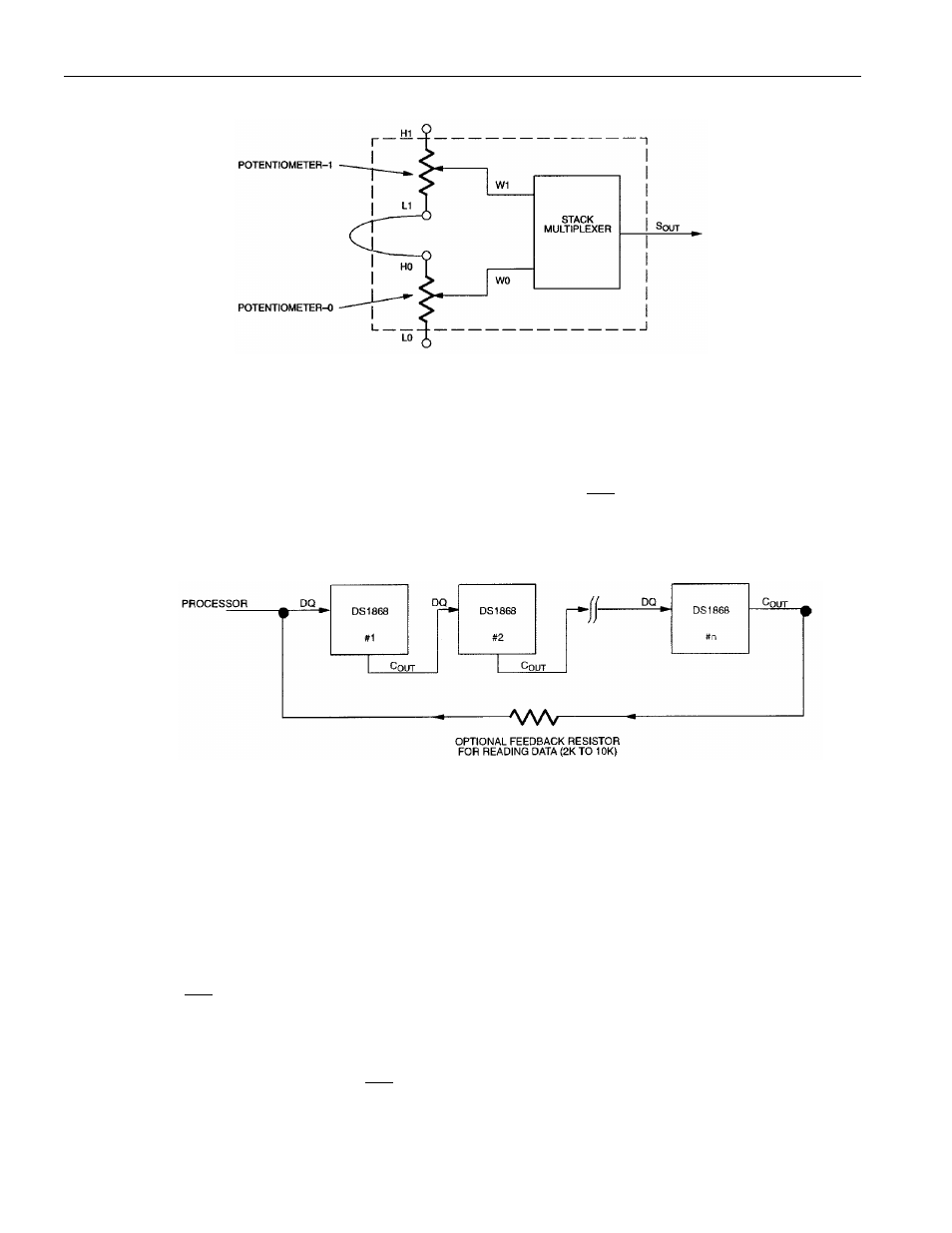
STACKED CONFIGURATION Figure 3
CASCADE OPERATION
A feature of the DS1868 is the ability to control multiple devices from a single processor. Multiple
DS1868s can be linked or daisy chained as shown in Figure 4. As a data bit is entered into the I/O shift
register of the DS1868 a bit will appear at the C
OUT
output after a minimum delay of 50 nanoseconds. The
stack select bit of the DS1868 will always be the first out the part at the beginning of a transaction. The
C
OUT
pin will always have the value of the stack select bit (b0) when
RST
is inactive.
CASCADING MULTIPLE DEVICES Figure 4
The C
OUT
output of the DS1868 can be used to drive the DQ input of another DS1868. When connecting
multiple devices, the total number of bits transmitted is always 17 times the number of DS1868s in the
daisy chain.
An optional feedback resistor can be placed between the C
OUT
terminal of the last device and the first
DS1868 DQ, input thus allowing the controlling processor to read, as well as, write data, or circularly
clock data through the daisy chain. The value of the feedback or isolation resistor should be in the range
from 2 to 10 kohms.
When reading data via the C
OUT
pin and isolation resistor, the DQ line is left floating by the reading
device. When
RST
is driven high, bit 17 is present on the C
OUT
pin, which is fed back to the input DQ
pin through the isolation resistor. When the CLK input transitions low to high, bit 17 is loaded into the
first position of the I/O shift register and bit 16 becomes present on C
OUT
and DQ of the next device. After
17 bits (or 17 times the number of DS1868s in the daisy chain), the data has shifted completely around
and back to its original position. When
RST
transitions to the low state to end data transfer, the value (the
same as before the read occurred) is loaded into the wiper-0, wiper-1, and stack select bit I/O register.