Capacitance (t, 25 °c), Ac electrical characteristics (-40 °c to +85°c; v – Rainbow Electronics DS1868 User Manual
Page 11: 0v ± 10%)
DS1868
11 of 14
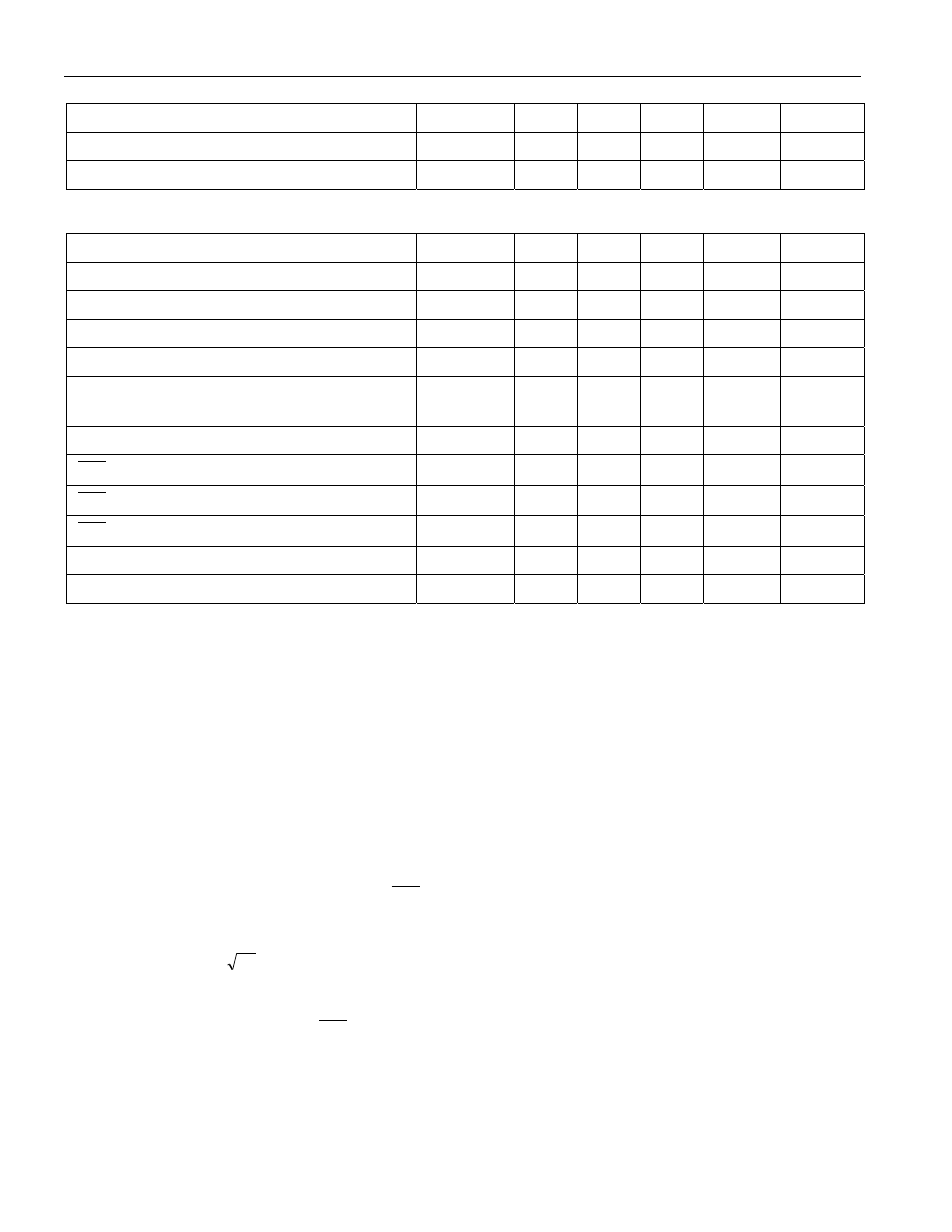
CAPACITANCE
(t
A
=25
°C)
PARAMETER
SYMBOL
MIN
TYP
MAX
UNITS
NOTES
Input Capacitance
C
IN
5
pF
3, 6
Output Capacitance
C
OUT
7
pF
3, 6
AC ELECTRICAL CHARACTERISTICS
(-40
°C to +85°C; V
CC
=5.0V
± 10%)
PARAMETER
SYMBOL
MIN
TYP
MAX
UNITS
NOTES
CLK Frequency
f
CLK
DC
10
MHz
10
Width of CLK Pulse
t
CH
50
ns
10
Data Setup Time
t
DC
30
ns
10
Data Hold Time
t
CDH
10
ns
10
Propagation Delay Time Low to High Level
Clock to Output
t
PLH
50
ns
10, 13
Propagation Delay Time High to Low Level
t
PLH
50
ns
10, 13
RST
High to Clock Input High
t
CC
50
ns
10
RST
Low from Clock Input High
t
HLT
50
ns
10
RST
Inactive
t
RLT
125
ns
10
Clock Low to Data Valid on a Read
t
CDD
30
ns
10
CLK Rise Time, CLK Fall Time
t
CR
50
ns
10
NOTES:
1. All voltages are referenced to ground.
2. Resistor inputs cannot exceed V
B
- 0.5V in the negative direction.
3. Capacitance values apply at 25
°C.
4. Absolute linearity is used to determine wiper voltage versus expected voltage as determined by wiper
position. Device test limits
±1.6 LSB.
5. Relative linearity is used to determine the change in voltage between successive tap positions. Device
test limits
±0.5 LSB.
6. Typical values are for t
A
= 25
°C and nominal supply voltage.
7. -3 dB cutoff frequency characteristics for the DS1868 depend on potentiometer total resistance:
DS1868-010; 1 MHz, DS1868-050; 200 kHz; and DS1868-100; 80 kHz.
8. Cout is active regardless of the state of
RST
.
9. V
REF
= 1.5 volts.
10. See Figure 9(a), (b), and (c).
11. Noise < -120 dB/
Hz
. Reference 1 volt (thermal).
12. Supply current is dependent on clock rate (see Figure 11).
13. See Figure 10.
14. Standby currents apply when
RST
, LLIC, DQ are in the low-state.
15. When biasing the substrate minimum V
B
= -3.0V
± 10% and maximum V
CC
= 3.0V
± 10%.
16. Valid at 25
°C only.