Pin description (continued) – Rainbow Electronics MAX8728 User Manual
Page 13
MAX8728
Low-Cost, Multiple-Output
Power Supply for LCD Monitors/TVs
______________________________________________________________________________________
13
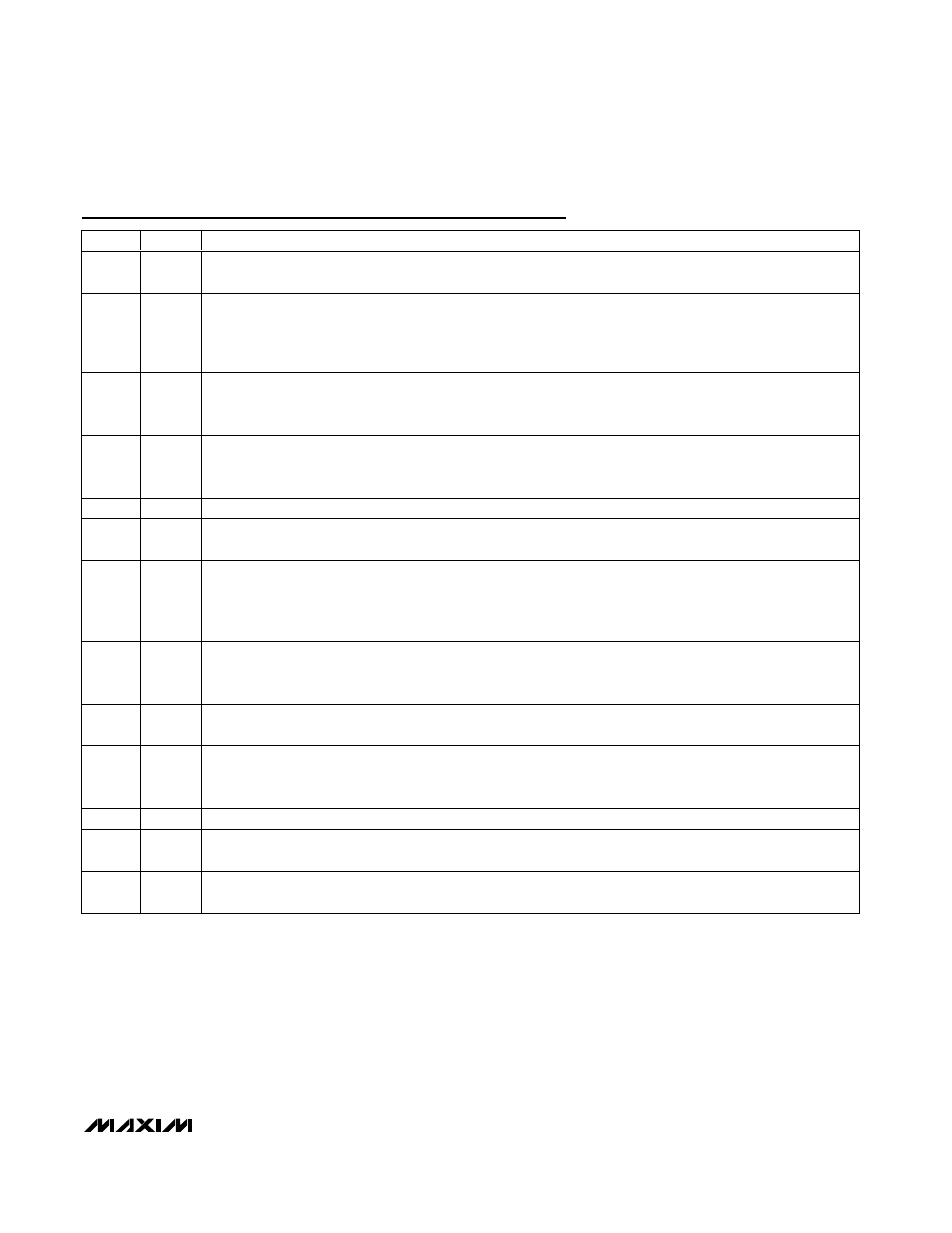
Pin Description (continued)
PIN
NAME
FUNCTION
21
DRN
High-Voltage Switch Control Input. DRN is the drain of the internal high-voltage p-channel MOSFET connected
to GON. See the High-Voltage Switch Control section for details.
22
THR
GON Falling Regulation Adjustment Input. Connect THR to the center of a resistive voltage-divider between a
reference supply and GND to adjust the GON falling regulation set point. CTL and MODE allow GON to
disconnect from SRC and be discharged through DRN; discharge stops when GON reaches 10 x V
THR
. See
the High-Voltage Switch Control section for details.
23
FB2
Step-Up Regulator Feedback Input. Connect FB2 to the center of a resistive voltage-divider between the step-
up regulator output and GND to set the step-up regulator output voltage. Place the resistive voltage-divider
close to FB2.
24
FBN
Negative Charge-Pump Regulator Feedback Input. Connect FBN to the center of a resistive voltage-divider
between the negative output and REF to set the negative charge-pump regulator output voltage. Place the
resistive voltage-divider close to FBN.
25
GND2
Step-Down Regulator Power Ground
26
LX2
Step-Up Regulator Switching Node. Connect the inductor and the Schottky diode to LX2 and minimize the
trace area for low EMI.
27
GATE
Input MOSFET Gate-Driver Output. GATE controls an external p-channel MOSFET between the input voltage
and the step-up regulator’s inductor. The switch is off when the step-up regulator is turned off, so that the
regulator’s output discharges to ground. During startup, the step-up regulator’s soft-start begins when V
GATE
falls below the GATE done threshold.
28
EN
Enable Input. Pulling EN high or leaving EN unconnected enables the step-up regulator and the negative
charge pump. Connecting EN to GND disables the above blocks and puts the step-down regulator in skip
mode. EN sources 5µA to allow a capacitor-controlled startup delay.
29
MODE
High-Voltage Switch-Control Block Mode Selection Input and Timing-Adjustment Input. See the High-Voltage
Switch Control section for details.
30
DEL
Positive Charge-Pump Regulator and High-Voltage Switch-Control Delay Input. Connect a capacitor between
DEL and GND to set the delay time. A 5µA current source charges C
DEL
. DEL is internally pulled to GND
through a 20
Ω internal resistor in shutdown.
31
COMP
Step-Up Regulator Error Amplifier Compensation Pin. See the Loop Compensation section for details.
32
FB1
Step-Down Regulator Feedback Input. Connect FB1 to the center of a resistive voltage-divider between the
step-down regulator output and GND to set the step-down regulator output voltage.
—
EP
Exposed Pad. Connect the exposed backside pad to GND and provide adequate thermal path to cool the IC.
See the PC Board Layout and Grounding section.