Pin description – Rainbow Electronics MAX8728 User Manual
Page 12
MAX8728
Low-Cost, Multiple-Output
Power Supply for LCD Monitors/TVs
12
______________________________________________________________________________________
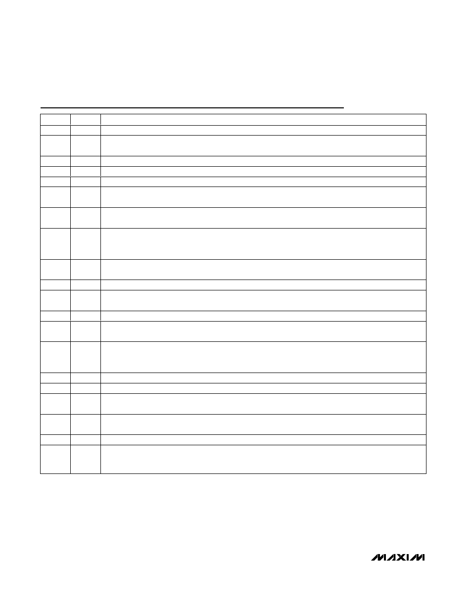
Pin Description
PIN
NAME
FUNCTION
1
GND1
Step-Down Regulator and Negative Charge-Pump Power Ground
2
OUT1
Step-Down Regulator Output Sense Input. OUT1 is the inverting input to the internal current-sense amplifier.
Connect OUT1 directly to the step-down regulator output.
3
DRVN
Negative Charge-Pump Regulator Driver Output. See the Negative Charge-Pump Regulator section for details.
4
CTL
High-Voltage Switch-Control Block Timing Control Input. See the High-Voltage Switch Control section for
5
IN
Step-Down Regulator and Negative Charge-Pump Regulator Supply Input
6
LX1
Step-Down Regulator Switching Node. LX1 is the source of the internal high-side MOSFET. Connect the
inductor and Schottky catch diode to LX1 and minimize the trace area for low EMI.
7
BST
Step-Down Regulator Bootstrap Pin. BST is the supply for the high-side MOSFET gate driver. Connect a 0.1µF
ceramic capacitor from BST to LX1.
8
INL
5V Internal Linear Regulator and Startup Circuitry Supply Input. The input voltage range of INL is between
+7.0V and +13.2V. Connect a 0.22µF ceramic capacitor between INL and GND. Place the capacitor close to
the IC.
9
VL
5V Internal Linear Regulator Output. VL powers the internal MOSFET gate drivers and the control circuitry.
Bypass VL
to GND with a 1µF ceramic capacitor. VL can provide up to 25mA external load current.
10
V
CC
Internal Reference Supply Input. Connect V
CC
directly to VL.
11
SHDN
Active-Low Shutdown Control Input. All outputs (except for REF and VL) are disabled and the GATE pin goes
high when
SHDN is low.
12
GND
Analog Ground
13
REF
Reference Output. Connect a 0.22µF ceramic capacitor between REF and GND. All regulator outputs are
disabled until REF exceeds its UVLO threshold.
14
FBP
Positive Charge-Pump Regulator Feedback Input. Connect FBP to the center of a resistive voltage-divider
between the positive output and GND to set the positive charge-pump regulator output voltage. Place the
resistive voltage-divider close to FBP.
15
GNDP
Positive Charge-Pump Power Ground
16
DRVP
Positive Charge-Pump Regulator Driver Output. See the Positive Charge-Pump Regulator section for details.
17
SUPP
Positive Charge-Pump Regulator Supply Input. Connect SUPP directly to IN and bypass SUPP to GNDP with a
minimum 0.1µF ceramic capacitor.
18
FSEL
Frequency Select Pin. Connect FSEL to REF for 500kHz operation. Connect FSEL to V
CC
for 1MHz operation.
Connect to GND for 1.5MHz operation.
19
SRC
High-Voltage Switch Control Block Input. SRC is the source of the internal, high-voltage, p-channel MOSFET.
20
GON
High-Voltage Switch Control Block Output. GON is the common junction of the internal high-voltage MOSFETs.
GON is internally pulled to GND through a 4mA internal current source when the switch control block is
disabled.