Ac electrical characteristics – Rainbow Electronics MAX9218 User Manual
Page 4
MAX9218
27-Bit, 3MHz-to-35MHz
DC-Balanced LVDS Deserializer
4
_______________________________________________________________________________________
Note 1: Current into a pin is defined as positive. Current out of a pin is defined as negative. All voltages are referenced to ground
except V
TH
and V
TL
.
Note 2: Maximum and minimum limits over temperature are guaranteed by design and characterization. Devices are production
tested at T
A
= +25°C.
Note 3: All LVTTL/LVCMOS inputs, except PWRDWN at
≤ 0.3V or ≥ V
CC
- 0.3V. PWRDWN is
≤ 0.3V.
Note 4: AC parameters are guaranteed by design and characterization, and are not production tested. Limits are set at
±6 sigma.
Note 5: C
L
includes probe and test jig capacitance.
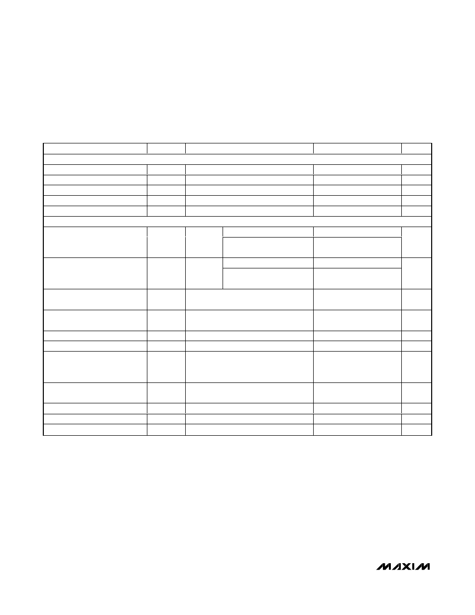
AC ELECTRICAL CHARACTERISTICS
(V
CC_
= +3.0V to 3.6V, C
L
= 8pF, PWRDWN = high, differential input voltage
⏐V
ID
⏐ = 0.1V to 1.2V, input common-mode voltage
V
CM
=
⏐V
ID
/2
⏐ to V
CC
-
⏐V
ID
/2
⏐, T
A
= -40°C to +85°C, unless otherwise noted. Typical values are at V
CC_
= +3.3V,
⏐V
ID
⏐ = 0.2V, V
CM
=
1.2V, T
A
= +25°C.) (Notes 4, 5)
PARAMETER
SYMBOL
CONDITIONS
MIN
TYP
MAX
UNITS
REFCLK TIMING REQUIREMENTS
Period
t
T
28.57
333.00
ns
Frequency
f
CLK
3
35
MHz
Frequency Variation
∆f
CLK
REFCLK to serializer PCLK_IN
-2.0
+2.0
%
Duty Cycle
DC
40
50
60
%
Transition Time
t
TRAN
20% to 80%
6
ns
SWITCHING CHARACTERISTICS
RNG1, RNG0 = high
3.2
4.4
Output Rise Time
t
R
Figure 3
RNG1, RNG0 both not high
simultaneously
3.8
5.5
ns
RNG1, RNG0 = high
2.7
4.5
Output Fall Time
t
F
Figure 3
RNG1, RNG0 both not high
simultaneously
3.6
5.3
ns
PCLK_OUT High Time
t
HIGH
Figure 4
0.4 x
t
T
0.45 x
t
T
0.6 x
t
T
ns
PCLK_OUT Low Time
t
LOW
Figure 4
0.4 x
t
T
0.45 x
t
T
0.6 x
t
T
ns
Data Valid Before PCLK_OUT
t
DVB
Figure 5
0.35 x t
T
0.4 x t
T
ns
Data Valid After PCLK_OUT
t
DVA
Figure 5
0.35 x t
T
0.4 x t
T
ns
Input-to-Output Delay
t
DELAY
Figure 6
2.575 x
t
T
+
8.5
2.725 x
t
T
+
12.8
ns
PLL Lock to REFCLK
t
PLLREF
Figure 7
16385 x
t
T
ns
Power-Down Delay
t
PDD
Figure 7
100
ns
Output Enable Time
t
OE
Figure 8
30
ns
Output Disable Time
t
OZ
Figure 9
30
ns