Rainbow Electronics MAX9218 User Manual
Page 13
MAX9218
27-Bit, 3MHz-to-35MHz
DC-Balanced LVDS Deserializer
______________________________________________________________________________________
13
Staggered and Transition Time Adjusted
Outputs
RGB_OUT[17:0] are grouped into three groups of six,
with each group switching about 1ns apart in the video
phase to reduce EMI and ground bounce.
CNTL_OUT[8:0] switch during the control phase. Output
transition times are slower in the 3MHz-to-7MHz and
7MHz-to-15MHz ranges and faster in the 15MHz-to-
35MHz range.
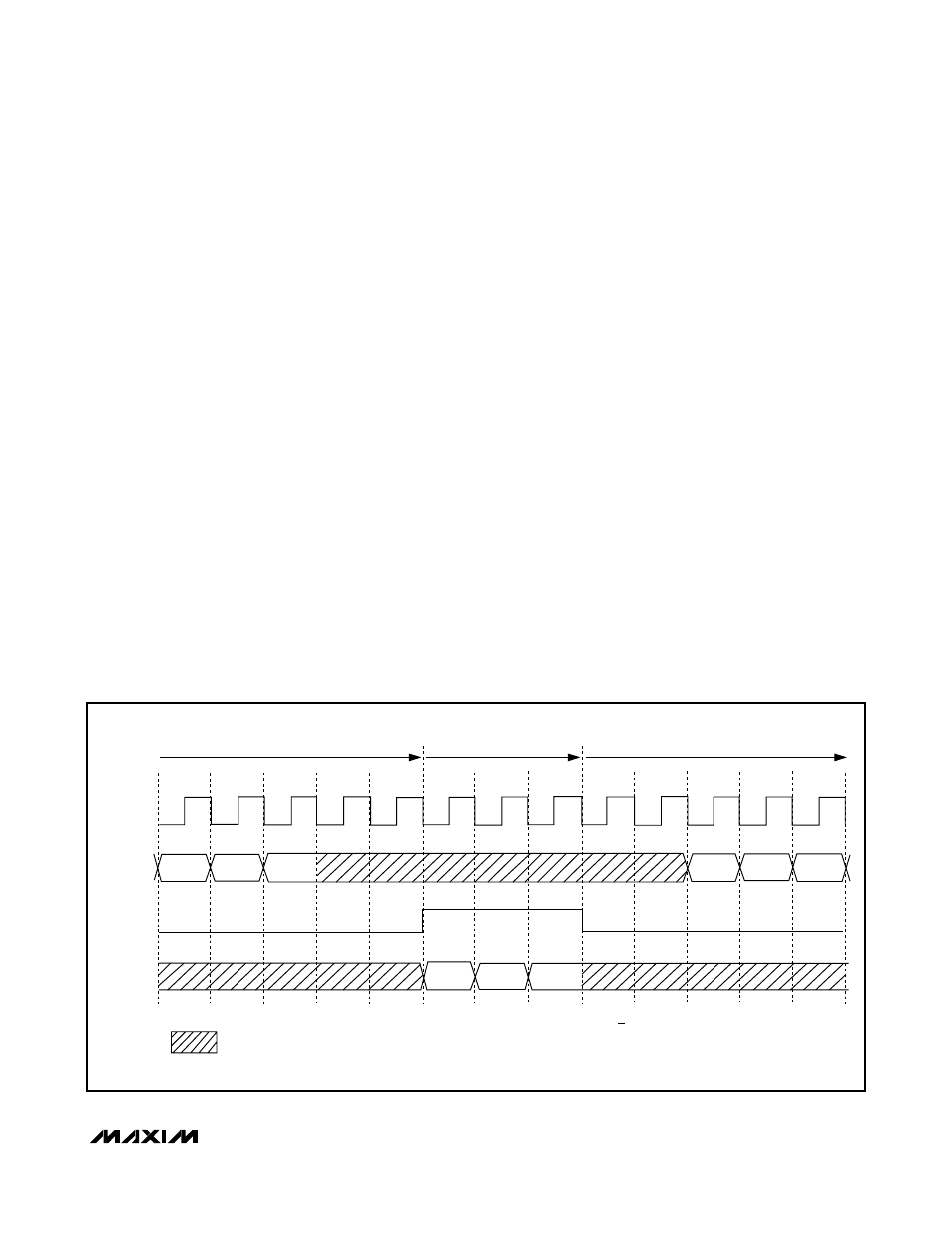
Data Enable Output (DE_OUT)
The MAX9218 deserializes video and control data at dif-
ferent times. Control data is deserialized during the video
blanking time. DE_OUT high indicates that video data is
being deserialized and output on RGB_OUT[17:0].
DE_OUT low indicates that control data is being deserial-
ized and output on CNTL_OUT[8:0]. When outputs are
not being updated, the last data received is latched on
the outputs. Figure 13 shows the DE_OUT timing.
Power-Supply Circuits and Bypassing
There are separate on-chip power domains for digital
circuits and LVTTL/LVCMOS inputs (V
CC
supply and
GND), outputs (V
CCO
supply and V
CCO
GND), PLL
(V
CCPLL
supply and V
CCPLL
GND), and the LVDS input
(V
CCLVDS
supply and V
CCLVDS
GND). The grounds are
isolated by diode connections. Bypass each V
CC
,
V
CCO
, V
CCPLL
, and V
CCLVDS
pin with high-frequency,
surface-mount ceramic 0.1µF and 0.001µF capacitors
in parallel as close to the device as possible, with the
smallest value capacitor closest to the supply pin. The
outputs are powered from V
CCO
, which accepts a
1.71V to 3.6V supply, allowing direct interface to inputs
with 1.8V to 3.3V logic levels.
Cables and Connectors
Interconnect for LVDS typically has a differential
impedance of 100
Ω. Use cables and connectors that
have matched differential impedance to minimize
impedance discontinuities.
Twisted-pair and shielded twisted-pair cables offer
superior signal quality compared to ribbon cable and
tend to generate less EMI due to magnetic field cancel-
ing effects. Balanced cables pick up noise as common
mode, which is rejected by the LVDS receiver.
Board Layout
Separate the LVTTL/LVCMOS outputs and LVDS inputs
to prevent crosstalk. A four-layer PC board with separate
layers for power, ground, and signals is recommended.
PCLK_OUT
CNTL_OUT
DE_OUT
RGB_OUT
= OUTPUT DATA HELD
PCLK_OUT TIMING SHOWN FOR R/F = HIGH (RISING OUTPUT LATCH EDGE)
CONTROL DATA
CONTROL DATA
VIDEO DATA
Figure 13. Output Timing