Pin description, Typical operating characteristics (continued) – Rainbow Electronics MAX13045E User Manual
Page 6
MAX13042E–MAX13045E
1.62V to 3.6V Improved High-Speed LLT
6
_______________________________________________________________________________________
Pin Description
PIN
UCSP
TDFN
NAME
FUNCTION
A1
8
I/O V
CC
4
Input/Output 4. Referenced to V
CC
.
A2
10
I/O V
CC
3
Input/Output 3. Referenced to V
CC
.
A3
12
I/O V
CC
2
Input/Output 2. Referenced to V
CC
.
A4
14
I/O V
CC
1
Input/Output 1. Referenced to V
CC
.
B1
9
V
CC
Power-Supply Voltage, +2.2V to +3.6V. Bypass V
CC
to GND with a
0.1µF ceramic capacitor. For full ESD protection, connect an
additional 1µF ceramic capacitor from V
CC
to GND as close to the
V
CC
input as possible.
B2
6
V
L
Logic Supply Voltage, +1.62V to +3.2V. Bypass V
L
to GND with a
0.1µF ceramic capacitor placed as close to the device as possible.
B3
2
EN
Enable Input. Drive EN to GND for shutdown mode, or drive EN to
V
L
or V
CC
for normal operation.
B4
13
GND
Ground
C1
7
I/O V
L
4
Input/Output 4. Referenced to V
L
.
C2
5
I/O V
L
3
Input/Output 3. Referenced to V
L
.
C3
3
I/O V
L
2
Input/Output 2. Referenced to V
L
.
C4
1
I/O V
L
1
Input/Output 1. Referenced to V
L
.
—
4, 11
N.C.
No Connection. Leave N.C. unconnected.
—
EP
EP
Exposed Pad. Connect exposed pad to GND.
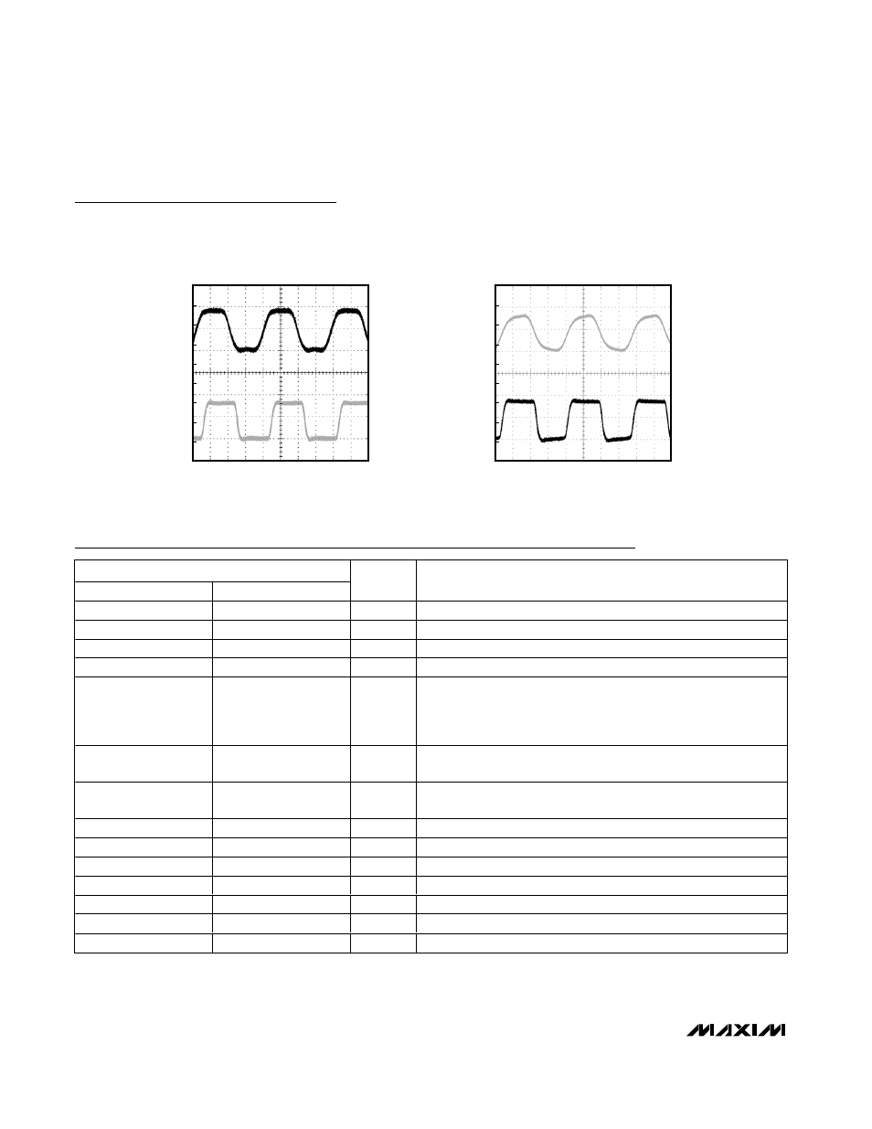
Typical Operating Characteristics (continued)
(V
CC
= 3.3V, V
L
= 1.8V, C
IOVCC_
= 10pF, C
IOVL_
= 15pF, R
SOURCE
= 150
Ω, data rate = 100Mbps, push-pull driver, T
A
= +25°C,
unless otherwise noted.)
TYPICAL I/O V
L_
DRIVING
(FREQUENCY = 26MHz, C
IOVCC_
= 40pF)
MAX1342E toc13
I/O V
L_
1V/div
I/O V
CC_
2V/div
10ns/div
TYPICAL I/O V
CC_
DRIVING
(FREQUENCY = 26MHz, C
IOVL_
= 15pF)
MAX1342E toc14
I/O V
L_
1V/div
I/O V
CC_
2V/div
10ns/div