Pin description – Rainbow Electronics MAX15046B User Manual
Page 8

40V, High-Performance, Synchronous
Buck Controller
MAX15046
8 ______________________________________________________________________________________
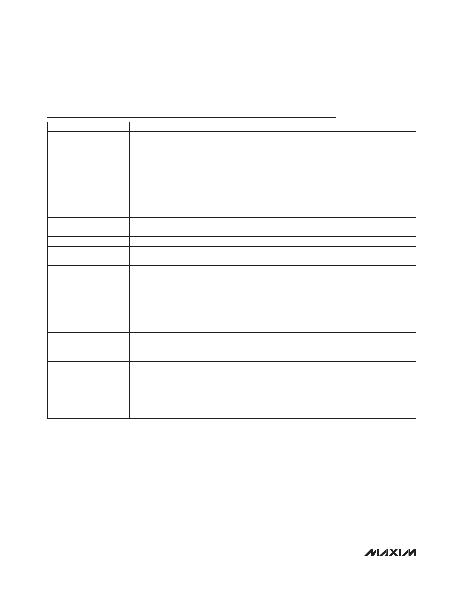
Pin Description
PIN
NAME
FUNCTION
1
IN
Regulator Input. Connect to the input rail of the buck converter. Bypass IN to PGND with a 100nF
minimum ceramic capacitor. When operating in the 5V Q10% range, connect IN to V
CC
.
2
V
CC
5.25V Linear Regulator Output. Bypass V
CC
to PGND with a ceramic capacitor of at least 4.7FF
when V
CC
supplies MOSFET gate-driver current at DRV or 2.2FF when V
CC
is not used to power
DRV.
3
PGOOD
Open-Drain Power-Good Output. Pull up PGOOD to an external power supply or output with an
external resistor.
4
EN
Active-High Enable Input. Pull EN to GND to disable the buck converter output. Connect to V
CC
for always-on operation. EN can be used for power sequencing and as a UVLO adjustment input.
5
LIM
Current-Limit Input. Connect a resistor from LIM to GND to program the current-limit threshold from
30mV (R
LIM
= 6kI) to 300mV (R
LIM
= 60kI).
6
COMP
Error-Amplifier Output. Connect compensation network from COMP to FB or from COMP to GND.
7
FB
Feedback Input (Inverting Input of Error Amplifier). Connect FB to a resistive divider between the
buck converter output and GND to adjust the output voltage from 0.6V up to 0.85 x IN.
8
RT
Oscillator-Timing Resistor Input. Connect a resistor from RT to GND to set the oscillator frequency
from 100kHz to 1MHz.
9
GND
Analog Ground. Connect PGND and AGND together at a single point.
10
PGND
Power Ground. Use PGND as a return path for the low-side MOSFET gate driver.
11
DRV
Gate-Driver Supply Voltage. DRV is internally connected to the low-side driver supply. Bypass DRV to
PGND with a 2.2FF minimum ceramic capacitor (see the Typical Application Circuits).
12
DL
Low-Side External MOSFET Gate-Driver Output. DL swings from DRV to PGND.
13
BST
Boost Flying Capacitor Connection. Internally connected to the high-side driver supply. Connect a
ceramic capacitor of at least 100nF between BST and LX and a diode between BST and DRV for
the high-side MOSFET gate-driver supply.
14
LX
Inductor Connection. Also serves as a return terminal for the high-side MOSFET driver current.
Connect LX to the switching side of the inductor.
15
DH
High-Side External MOSFET Gate-Driver Output. DH swings from BST to LX.
16
CSP
Current-Sense Positive Input. Connect to the drain of low-side MOSFET with Kelvin connection.
—
EP
Exposed Pad. EP is internally connected to ground. Connect EP to a large copper ground plane to
maximize thermal performance.
