Rainbow Electronics MAX15046B User Manual
Page 19
40V, High-Performance, Synchronous
Buck Controller
MAX15046
______________________________________________________________________________________ 19
overall thermal budget. Ensure that the DL gate driver
can drive the low-side MOSFET. In particular, check
that the dv/dt caused by the high-side MOSFET turning
on does not pull up the low-side MOSFET gate through
the drain-to-gate capacitance of the low-side MOSFET,
which is the most frequent cause of crossconduction
problems.
Check power dissipation when using the internal linear
regulator to power the gate drivers. Select MOSFETs
with low gate charge so that V
CC
can power both drivers
without overheating the device:
P
DRIVE
= V
CC
x Q
G_TOTAL
x f
SW
where Q
G_TOTAL
is the sum of the gate charges of the
two external MOSFETs.
Boost Capacitor and Diode Selection
The MAX15046 uses a bootstrap circuit to generate
the necessary gate-to-source voltage to turn on the
high-side MOSFET. The selected n-channel high-side
MOSFET determines the appropriate boost capacitance
value (C
BST
in the Typical Application Circuits) accord-
ing to the following equation:
=
∆
G
BST
BST
Q
C
V
where Q
G
is the total gate charge of the high-side
MOSFET and DV
BST
is the voltage variation allowed
on the high-side MOSFET driver after turn-on. Choose
D
V
BST
such that the available gate-drive voltage is not
significantly degraded (e.g. DV
BST
= 100mV to 300mV)
when determining C
BST
.
Use a low-ESR ceramic capacitor as the boost capacitor
with a minimum value of 100nF.
A small-signal diode can be used for the bootstrap cir-
cuit and must have a minimum voltage rating of V
IN
+
3V to withstand the maximum BST voltage. The average
forward current of the diode should meet the following
requirement:
I
F
> Q
GATE
x f
SW
where Q
GATE
is the gate charges of the low-side MOSFET.
Power Dissipation
The maximum power dissipation of the device depends
on the thermal resistance from the die to the ambient
environment and the ambient temperature. The thermal
resistance depends on the device package, PCB copper
area, other thermal mass, and airflow.
The power dissipated into the package (P
T
) depends
on the supply configuration (see the Typical Application
Circuits). Use the following equation to calculate power
dissipation:
P
T
= V
IN
x [Q
G_TOTAL
x f
SW
+ I
Q
]
where I
Q
is the quiescent supply current at the switching
frequency. See the I
IN
vs. Switching Frequency graph in
the Typical Operating Characteristics for the I
Q
.
Use the following equation to estimate the temperature
rise of the die:
T
J
= T
A
+ (P
T
x B
JA
)
where B
JA
is the junction-to-ambient thermal impedance
of the package, P
T
is power dissipated in the device,
and T
A
is the ambient temperature. The B
JA
is 103.7NC/W
for the 16-pin QSOP and 53NC/W for the 16-pin QSOP-
EP package on multilayer boards, with the conditions
specified by the respective JEDEC standards (JESD51-5,
JESD51-7). An accurate estimation of the junction tem-
perature requires a direct measurement of the case
temperature (T
C
) when actual operating conditions
significantly deviate from those described in the JEDEC
standards. The junction temperature is then:
T
J
= T
C
+ (P
T
x B
JC
)
Use 37NC/W as B
JC
thermal impedance for the 16-pin
QSOP package and 6NC/W for the 16-pin QSOP-EP
package. The case-to-ambient thermal impedance (B
CA
)
is dependent on how well the heat is transferred from the
PCB to the ambient. Use large copper areas to keep the
PCB temperature low.
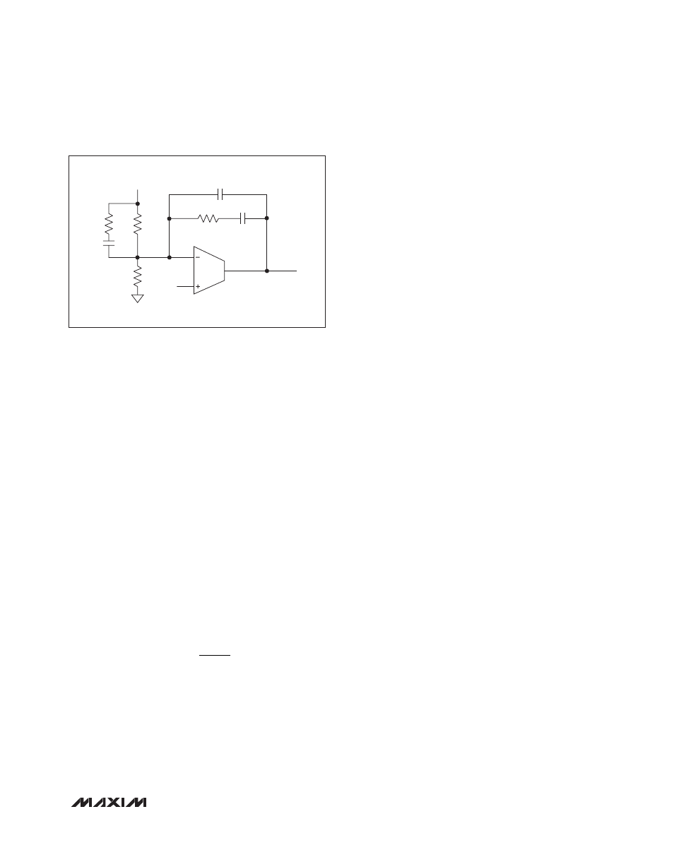
Figure 4. Type III Compensation Network
V
REF
g
M
R
1
R
2
V
OUT
R
I
COMP
C
I
C
CF
R
F
C
F