Applications information – Rainbow Electronics MAX15046B User Manual
Page 13

40V, High-Performance, Synchronous
Buck Controller
MAX15046
______________________________________________________________________________________ 13
MAX15046 stops both DL and DH drivers and waits for
4096 switching cycles (hiccup timeout delay) before
attempting a new soft-start sequence. The hiccup-mode
protection remains active during the soft-start time.
Undervoltage Lockout
The MAX15046 provides an internal undervoltage lock-
out (UVLO) circuit to monitor the voltage on V
CC
. The
UVLO circuit prevents the MAX15046 from operating
when V
CC
is lower than V
UVLO
. The UVLO threshold is
4V, with 400mV hysteresis to prevent chattering on the
rising/falling edge of the supply voltage. DL and DH stay
low to inhibit switching when the device is in undervolt-
age lockout.
Thermal-Overload Protection
Thermal-overload protection limits total power dissipa-
tion in the MAX15046. When the junction temperature of
the device exceeds +150NC, an on-chip thermal sensor
shuts down the device, forcing DL and DH low, which
allows the device to cool. The thermal sensor turns the
device on again after the junction temperature cools by
20NC. The regulator shuts down and soft-start resets
during thermal shutdown. Power dissipation in the LDO
regulator and excessive driving losses at DH/DL trigger
thermal-overload protection. Carefully evaluate the total
power dissipation (see the Power Dissipation section) to
avoid unwanted triggering of the thermal-overload pro-
tection in normal operation.
Applications Information
Effective Input-Voltage Range
The MAX15046 operates from 4.5V to 40V input supplies
and regulates output down to 0.6V. The minimum voltage
conversion ratio (V
OUT
/V
IN
) is limited by the minimum
controllable on-time. For proper fixed-frequency PWM
operation, the voltage conversion ratio must obey the
following condition:
OUT
ON(MIN)
SW
IN
V
t
f
V
>
×
where t
ON(MIN)
is 125ns and f
SW
is the switching fre-
quency in Hertz. Pulse skipping occurs to decrease the
effective duty cycle when the desired voltage conversion
does not meet the above condition. Decrease the switch-
ing frequency or lower the input voltage V
IN
to avoid
pulse skipping.
The maximum voltage conversion ratio is limited by the
maximum duty cycle (D
max
):
Ч
+
Ч
<
OUT
max
DROP2
max
DROP1
max
IN
IN
V
D
V
(1-D
) V
D
-
V
V
where V
DROP1
is the sum of the parasitic voltage drops
in the inductor discharge path, including synchronous
rectifier, inductor, and PCB resistance. V
DROP2
is the
sum of the resistance in the charging path, including
high-side switch, inductor, and PCB resistance. In prac-
tice, provide adequate margin to the above conditions
for good load-transient response.
Setting the Output Voltage
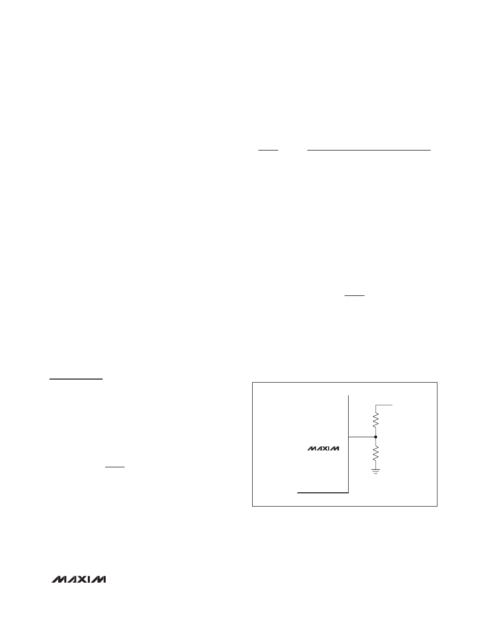
Set the MAX15046 output voltage by connecting a resis-
tive divider from the output to FB to GND (Figure 2).
Select R
2
from between 4kI and 16kI. Calculate R
1
with the following equation:
=
OUT
1
2
FB
V
R
R
-1
V
where V
FB
= 0.59V (see the Electrical Characteristics
table) and V
OUT
can range from 0.6V to (0.85 O V
IN
).
Resistor R
1
also plays a role in the design of the Type
III compensation network. Review the values of R
1
and
R
2
when using a Type III compensation network (see the
Type III Compensation Network (Figure 4) section).
Figure 2. Adjustable Output Voltage
FB
R
1
OUT
R
2
MAX15046
