Rainbow Electronics MAX15046B User Manual
Page 17
40V, High-Performance, Synchronous
Buck Controller
MAX15046
______________________________________________________________________________________ 17
The total loop gain, which is the product of the modulator
gain and the error-amplifier gain at f
O
, is:
(
)
MOD
EA
IN
FB
M
F
OSC
O
OUT
OUT
F
OSC
O
OUT
OUT
F
FB
IN
M
1) GAIN
GAIN
1
So :
V
V
ESR
g
R
1
V
(2
f
L
) V
Solving for R :
V
2
f
L
V
R
V
V
g
ESR
Ч
=
Ч
Ч
Ч
Ч
=
π Ч
Ч
Ч π Ч
Ч
Ч
=
Ч
Ч
Ч
2) Set a midband zero (f
Z1
) at 0.75 x f
PO
(to cancel one
of the LC poles):
=
=
×
π Ч
Ч
Z1
PO
F
F
1
f
0.75 f
2
R
C
Solving for C
F
:
=
π Ч
Ч
Ч
F
F
PO
1
C
2
R
f
0.75
3) Place a high-frequency pole at f
P1
= 0.5 x f
SW
(to
attenuate the ripple at the switching frequency f
SW
)
and calculate C
CF
using the following equation:
=
π Ч
Ч
CF
F
SW
F
1
C
1
R
f
-
C
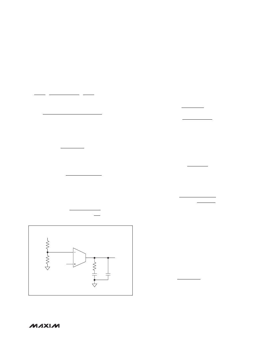
Type III Compensation Network
(See Figure 4)
When using a low-ESR tantalum or ceramic type, the
ESR-induced zero frequency is usually above the tar-
geted zero crossover frequency (f
O
). Use Type III com-
pensation. Type III compensation provides two zeros
and three poles at the following frequencies:
=
π Ч
Ч
=
π Ч
Ч
+
Z1
F
F
Z2
I
1
I
1
f
2
R
C
1
f
2
C (R
R )
Two midband zeros (f
Z1
and f
Z2
) cancel the pair of com-
plex poles introduced by the LC filter:
f
P1
= 0
f
P1
introduces a pole at zero frequency (integrator) for
nulling DC output-voltage errors:
=
π Ч
Ч
P2
I
I
1
f
2
R C
Depending on the location of the ESR zero (f
ZO
), use f
P2
to cancel f
ZO
, or to provide additional attenuation of the
high-frequency output ripple:
=
×
π Ч
Ч
+
P3
F
CF
F
F
CF
1
f
C
C
2
R
C
C
f
P3
attenuates the high-frequency output ripple.
Place the zeros and poles such that the phase margin
peaks around f
O
.
Ensure that R
F
>> 2/g
M
and the parallel resistance of
R
1
, R
2
, and R
I
is greater than 1/g
M
. Otherwise, a 180N
phase shift is introduced to the response making the
loop unstable.
Use the following compensation procedures:
1) With R
F
>> 10kI, place the first zero (f
Z1
) at 0.8 x
f
PO
:
=
=
×
π Ч
Ч
Z1
PO
F
F
1
f
0.8 f
2
R
C
Figure 3. Type II Compensation Network
V
REF
R
1
V
OUT
R
2
g
M
R
F
COMP
C
F
C
CF