Detailed description, Table 1. vid0 and vid1 configuration – Rainbow Electronics MAX8649 User Manual
Page 11
MAX8649
1.8A Step-Down Regulator with Differential
Remote Sense in 2mm x 2mm WLP
______________________________________________________________________________________
11
I
2
C INTERFACE
VOLTAGE
CONTROL, V
REF
,
BIAS, ETC.
PWM LOGIC
CLOCK GEN
OSC
V
DAC
SNS-
SNS+
PGND
LX
IN2
AGND
VID2
VID1
EN
IN1
SDA
SCL
V
DD
SYNC
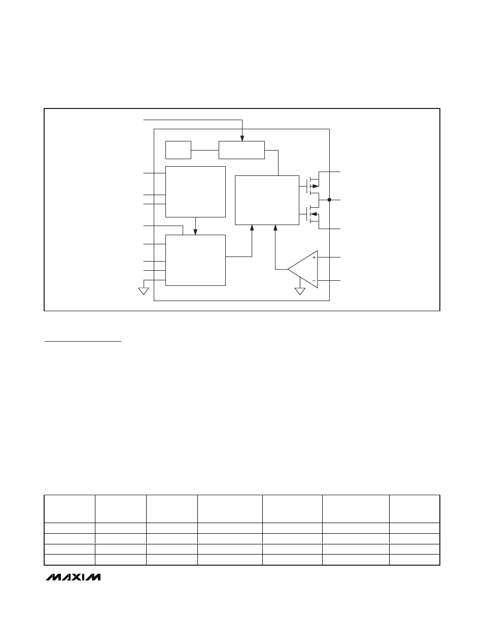
Figure 1. Block Diagram
Detailed Description
The MAX8649 high-efficiency, 3.25MHz step-down
switching regulator delivers up to 1.8A of output cur-
rent. The device operates from a 2.5V to 5.5V input
voltage range, and the output voltage is I
2
C program-
mable from 0.75V to 1.38V in 10mV increments. Fully
differential remote sense ensures precise DC regula-
tion at the load. Total output error is less than 2% over
load, line, and temperature.
Dynamic Voltage Scaling
The output voltage is dynamically adjusted by use of
the VID0 and VID1 logic inputs, allowing selection
between four predefined operation modes/voltage
configurations.
For each of the different output modes, the following
parameters are programmable:
•
Output voltage from 0.75V to 1.38V in 10mV steps
•
Mode of operation: Forced PWM or power save
•
Enable/disable of synchronization of switching
frequency to external clock source
The relation between the VID0/VID1 and operation
mode is given by Table 1.
The VID_ inputs have internal pulldown resistors. These
pulldown resistors can be disabled through the CONTROL
register after the MAX8649 is enabled, achieving low-
est possible quiescent current. When EN is low, the
CONTROL register is reset to default, enabling the pull-
down resistors (see Table 7).
VID0
VID1
MODE
I
2
C REGISTER
DEFAULT
SWITHCING
MODE
DEFAULT
SYN C H R O N IZ A TIO N
DEFAULT
OUTPUT
VOLTAGE (V)
0
0
MODE0
Table 3
FORCED PWM
OFF
1.27
0
1
MODE1
Table 4
POWER SAVE
OFF
1.05
1
0
MODE2
Table 5
FORCED PWM
OFF
1.22
1
1
MODE3
Table 6
FORCED PWM
OFF
1.05
Table 1. VID0 and VID1 Configuration