Absolute maximum ratings, Dc electrical characteristics–dual supplies – Rainbow Electronics MAX14753 User Manual
Page 2
MAX14752/MAX14753
8-Channel/Dual 4-Channel
72V Analog Multiplexers
2
_______________________________________________________________________________________
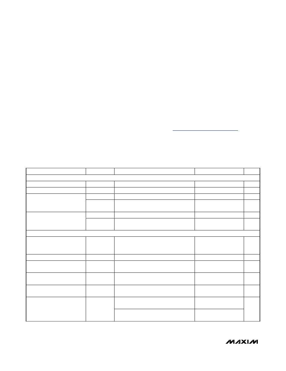
ABSOLUTE MAXIMUM RATINGS
Stresses beyond those listed under “Absolute Maximum Ratings” may cause permanent damage to the device. These are stress ratings only, and functional
operation of the device at these or any other conditions beyond those indicated in the operational sections of the specifications is not implied. Exposure to
absolute maximum rating conditions for extended periods may affect device reliability.
V
DD
to V
SS
.............................................................-0.3V to +72V
GND to V
SS
..............................................................-0.3V to V
DD
EN, S0, S1, S2 to GND .................................................................
..............................-0.3V to the lesser of (+12V and V
DD
+ 0.3V)
IN_, INA_, INB_, OUT, OUTA, OUTB to V
SS ......................................
...........
-2V to (V
DD
- V
SS
+ 2V) or 100mA (whichever occurs first)
Signal Slew Rate of IN_, INA_, INB_,
OUT, OUTA, OUTB ................................see SOA in Figure 11
Continuous Current into IN_, INA_,
INB_, OUT, OUTA, OUTB .............................................100mA
Continuous Power Dissipation (T
A
= +70°C)
16-Pin TSSOP (derate 11.1mW/°C above +70°C) ......890mW
Junction-to-Ambient Thermal Resistance (
θ
JA
) (Note 1)
16-Pin TSSOP ..............................................................90°C/W
Junction-to-Case Thermal Resistance (
θ
JC
) (Note 1)
16-Pin TSSOP ..............................................................27°C/W
Maximum Operating Temperature Range .........-40°C to +125°C
Junction Temperature ..................................................... +150°C
Storage Temperature Range .............................-65°C to +150°C
Lead Temperature (soldering, 10s) .................................+300°C
DC ELECTRICAL CHARACTERISTICS–DUAL SUPPLIES
(V
DD
= +35V, V
SS
= -35V, V
GND
= 0, V
EN
= +3.3V, T
A
= -40°C to +85°C, unless otherwise noted. Typical values are at T
A
= +25°C.)
PARAMETER
SYMBOL
CONDITIONS
MIN
TYP
MAX
UNITS
POWER SUPPLY
V
DD
Supply Voltage Range
V
DD
+10
+36
V
V
SS
Supply Voltage Range
V
SS
-10
-36
V
I
DD(OFF)
V
EN
= V
S_
= 0, V
IN_
=
V
INA_
= V
INB_
= +20V
12
25
µA
V
DD
Supply Current
I
DD(ON)
V
EN
= +5V, V
S_
= 0 or V
EN
, V
IN_
=
V
INA_
=
V
INB_
= +20V
270
600
mA
I
SS(OFF)
V
EN
= V
S_
= 0, V
IN_
=
V
INA_
= V
INB_
= +20V
11
25
µA
V
SS
Supply Current
I
SS(ON)
V
EN
= +5V, V
S_
= 0 or V
EN
, V
IN_
=
V
INA_
=
V
INB_
= +20V
260
600
mA
ANALOG MUX
Analog Signal Range
V
IN
, V
INA_,
V
INB_
, V
OUT,
V
OUTA,
V
OUTB
V
SS
V
DD
V
Current Through Multiplexer
I
IN,
I
INA,
I
INB,
V
IN_
, V
INA_
, V
INB_
= ±20V
-5
+5
mA
On-Resistance
R
ON
I
IN_,
I
INA_,
I
INB_
= 5mA; V
IN_
, V
INA_
, V
INB_
,
V
OUT
, V
OUTA
, V
OUTB
= ±20V, Figure 1
60
130
Ω
On-Resistance Matching
Between Channels
ΔR
ON
I
IN_,
I
INA_,
I
INB_
= 5mA, V
IN_
, V
INA_
, V
INB_
=
±20V, 0
0.5
Ω
On-Resistance Flatness
R
FLAT_(ON)
I
IN_,
I
INA_,
I
INB_
= 5mA, V
IN_
, V
INA_
, V
INB_
,
V
OUT
, V
OUTA
, V
OUTB
= ±20V
0.03
Ω
MAX14752: V
OUT
, V
OUTA
, V
OUTB
= ±20V,
V
IN_
, V
INA_
, V
INB_
= unconnected, Figure 2
-20
+20
Output On-Leakage Current
I
OUT(ON)
MAX14753: V
OUT
, V
OUTA
, V
OUTB
= ±20V,
V
IN_
, V
INA_
, V
INB_
= unconnected, Figure 2
-10
+10
nA
Note 1: Package thermal resistances were obtained using the method described in JEDEC specification JESD51-7, using a four-layer
board. For detailed information on package thermal considerations, refer to
www.maxim-ic.com/thermal-tutorial
.