Rainbow Electronics MAX9595 User Manual
Page 15

To implement the zero-crossing function when switch-
ing audio signals, set the ZCD bit by loading register
00h through the I
2
C-compatible interface (if the ZCD bit
is not already set). Then set the mute bit low by loading
register 00h. Next, wait for a sufficient period of time for
the audio signal to cross zero. This period is a function
of the audio signal path’s low-frequency 3dB corner
(f
L3dB
). Thus, if f
L3dB
= 1kHz, the time period to wait for
a zero-crossing detect is 0.5kHz or 0.5ms.
Next, set the appropriate TV switches using register
01h. Finally, clear the mute bit (while leaving the ZCD
bit high) using register 00h. The MAX9595 switches the
signal out of mute at the next zero crossing.
To implement the zero-cross function for TV volume
changes, or for TV and phono volume bypass switch-
ing, simply ensure the ZCD bit in register 00h is set.
Volume Control
The TV channel volume control ranges from -56dB to
+6dB in 2dB steps. The VCR volume control settings
are programmable for -6dB, 0dB, and +6dB. These
gain levels are referenced to the application inputs,
where some dividers are present. With the ZCD bit set,
the TV volume control switches only at zero-crossings,
thus minimizing click noise. The TV outputs can bypass
the volume control. Likewise, the monaural output sig-
nal can be processed by the TV volume control or it
can bypass the volume control.
Digital Section
Serial Interface
The MAX9595 uses a simple 2-wire serial interface
requiring only two standard microprocessor port I/O
lines. The fast-mode I
2
C-compatible serial interface
allows communication at data rates up to 400kbps or
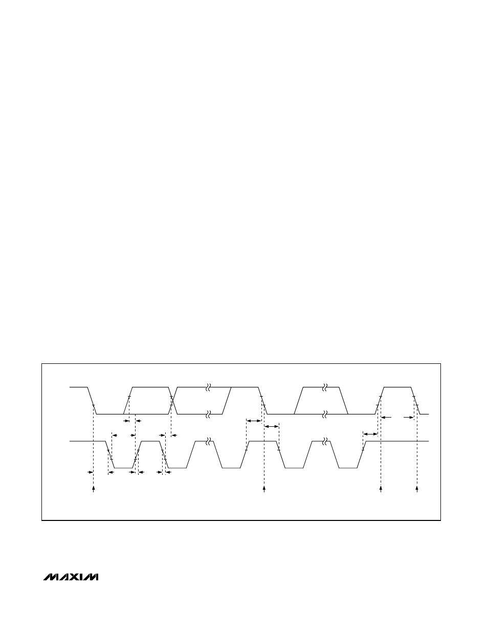
400kHz. Figure 4 shows the timing diagram of the sig-
nals on the 2-wire interface.
The two bus lines (SDA and SCL) must be at logic-high
when the bus is not in use. The MAX9595 is a slave
device and must be controlled by a master device.
Pullup resistors from the bus lines to the supply are
required when push-pull circuitry is not driving the
lines.
The logic level on the SDA line can only change when
the SCL line is low. The start and stop conditions occur
when SDA toggles low/high while the SCL line is high
(see Figure 5). Data on SDA must be stable for the
duration of the setup time (t
SU,DAT
) before SCL goes
high. Data on SDA is sampled when SCL toggles high
with data on SDA stable for the duration of the hold
time (t
HD,DAT
). Note that data is transmitted in an 8-bit
byte. A total of nine clock cycles are required to trans-
fer a byte to the MAX9595. The device acknowledges
the successful receipt of the byte by pulling the SDA
line low during the 9th clock cycle.
MAX9595
Audio/Video Switch for Dual SCART Connector
______________________________________________________________________________________
15
SCL
SDA
t
LOW
t
F
t
R
t
HD,STA
t
HD,DAT
t
HD,STA
t
SU,DAT
t
SU,STA
t
BUF
t
SU,STA
STOP CONDITION
REPEATED START CONDITION
START CONDITION
Figure 4. SDA and SCL Signal Timing Diagram
