Exposure time reduction – Rainbow Electronics TH7814A User Manual
Page 5
5
TH7813A/TH7814A
1990A–IMAGE–05/02
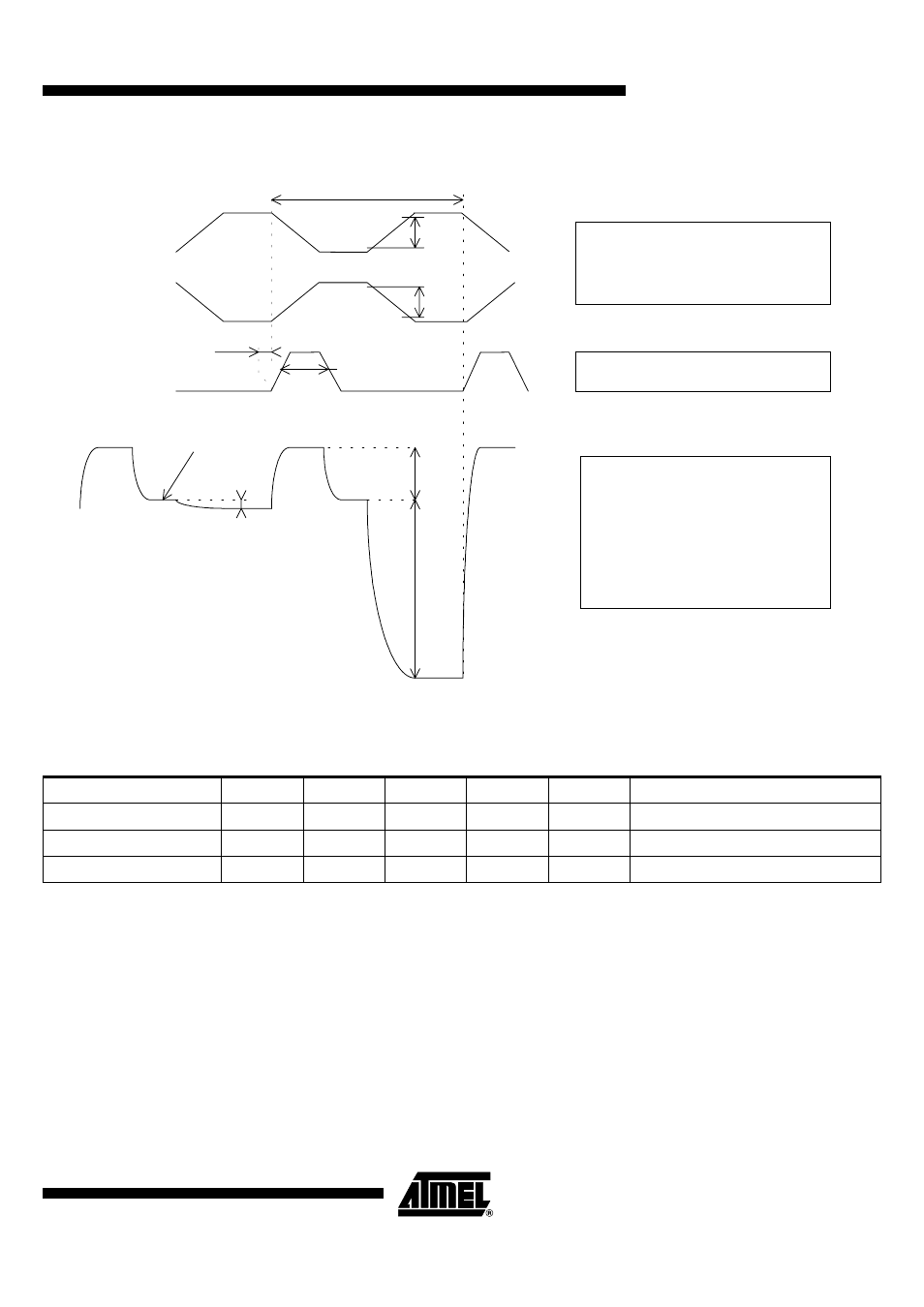
Figure 5. Pixel Readout Timing Diagram
Exposure Time
Reduction
The antiblooming structure of the TH7813A and TH7814A provides an electronic shutter
capability by clocking phase fA during the line period. The timing diagram is described
below:
Note:
Clock capacitance: TH7813A = 50 pF, TH7814A = 100 pF
L1
L2
R
10%
90%
90%
10%
tr
tf
Tpixel
0 ns
10 ns
50%
Video signal
Reset Feedthrough
Offset in darkness
VIDEO OUTPUTS
±
floating diode level
Duty cycle: 50%
±
10%
Crossover at 50%
±
10%
Rise and fall time
10 ns
Rise and fall time
8 ns
Video outputs are synchronous
Video signal occurs on L2 falling edge
First useful pixel occurs on 5th
falling edge of L2 after P
Antiblooming Gate
Φ
A
Min
Typ
Max
Unit
Clock Capacitance (see note)
High Level
8.5
9
9.5
V
Low Level Sets Saturation Level
Low Level
2
4
7
V
See Pixel Saturation Adjustment
Pulse Min.
200
ns