Applications information, Enable function, Differential inputs – Rainbow Electronics MAX9395 User Manual
Page 7: Power-supply bypassing, Differential traces, Output termination, Cables and connectors
back function. The loopback function routes the input of
channel A to the output of channel B, and the inputs of
channel B to the outputs of channel A. See Tables 1
and 2 for a summary of the input/output routing
between channels.
Enable Function
The EN_ _ logic inputs enable and disable each set of
differential outputs. Connect EN_ 0 to V
CC
to enable the
OUT_0/OUT_0 differential output pair. Connect EN_0 to
GND to disable the OUT_0/OUT_0 differential output
pair. The differential output pairs assert to a differential
low condition when disabled.
Applications Information
Differential Inputs
The MAX9394/MAX9395 inputs accept any differential
signaling standard within the specified common-mode
voltage range. The fail-safe feature detects common-
mode input signal levels and generates a differential
output low condition for undriven inputs or when the
common-mode voltage exceeds the specified range
(V
CM
≥ V
CC
- 0.6V, MAX9394; V
CM
≤ 0.6V, MAX9395).
Leave unused inputs unconnected or connect to V
CC
for the MAX9394 or to GND for the MAX9395.
Power-Supply Bypassing
Bypass each V
CC
to GND with high-frequency surface-
mount ceramic 0.1µF and 0.01µF capacitors in parallel
as close to the device as possible. Install the 0.01µF
capacitor closest to the device.
Differential Traces
Input and output trace characteristics affect the perfor-
mance of the MAX9394/MAX9395. Connect each input
and output to a 50
Ω characteristic impedance trace.
Maintain the distance between differential traces and
eliminate sharp corners to avoid discontinuities in dif-
ferential impedance and maximize common-mode
noise immunity. Minimize the number of vias on the dif-
ferential input and output traces to prevent impedance
discontinuities. Reduce reflections by maintaining the
50
Ω characteristic impedance through connectors and
across cables. Minimize skew by matching the electri-
cal length of the traces.
Output Termination
Terminate LVDS outputs with a 100
Ω resistor between
the differential outputs at the receiver inputs. LVDS out-
puts require 100
Ω termination for proper operation.
Ensure that the output currents do not exceed the cur-
rent limits specified in the Absolute Maximum Ratings.
Observe the total thermal limits of the MAX9394/
MAX9395 under all operating conditions.
Cables and Connectors
Use matched differential impedance for transmission
media. Use cables and connectors with matched differ-
ential impedance to minimize impedance discontinu-
ities. Avoid the use of unbalanced cables.
MAX9394/MAX9395
2:1 Multiplexers and 1:2 Demultiplexers with
Loopback
_______________________________________________________________________________________
7
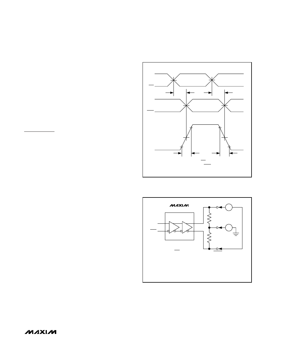
t
PHL
t
PLH
80%
20%
20%
80%
50%
V
OD
= 0V
V
OD
= 0V
V
ID
= 0V
V
OD
= 0V
V
OD
= 0V
V
ID
= 0V
50%
V
ID
= V
IN_ _
- V
IN_ _
V
OD
= V
OUT_ _
- V
OUT_ _
V
IN_ _
V
IHD
V
ILD
V
IN_ _
V
OUT_ _
V
OUT_ _
t
F
t
R
Figure 1. Output Transition Time and Propagation Delay Timing
Diagram
V
ID
= V
IN_ _
- V
IN_ _
∆V
OD
=
V
OD
- V
OD
*
R
L
= 100
Ω ±1%
∆V
OS
=
V
OS
- V
OS
*
V
OD
AND V
OS
ARE MEASURED WITH V
ID
= +100mV.
V
OD
* AND V
OS
*
ARE MEASURED WITH V
ID
= -100mV.
IN_ _
IN_ _
R
L
/2
R
L
/2
V
OD
OUT_ _
OUT_ _
MAX9394/MAX9395
EN_ _ = HIGH
V
OS
Figure 2. Test Circuit for V
OD
and V
OS