Rainbow Electronics MAX3028 User Manual
Page 7
MAX13013–MAX13017/MAX3023–MAX3028
+1.2V to +3.6V, 0.1µA, 100Mbps,
Single-/Dual-/Quad-Level Translators
_______________________________________________________________________________________
7
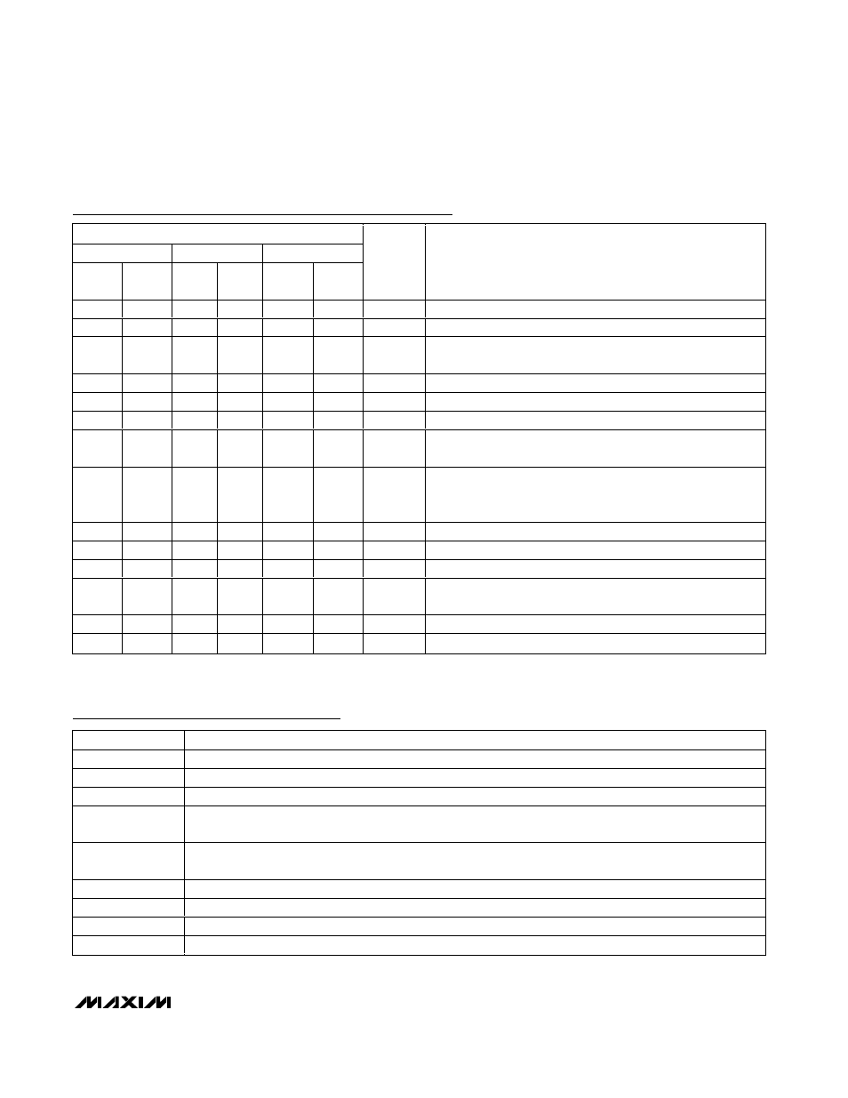
Pin Description—MAX13013/MAX13014/
MAX3023 (Bidirectional Devices)
PIN
MAX3023
MAX13013
MAX13014
TSSOP
4 x 3
UCSP
SC70
3 x 2
UCSP
SOT23
3 x 3
UCSP
NAME
FUNCTION
1
A1
4
B2
7
A2
I/O V
L
1
Input/Output 1, Referenced to V
L
2
B2
—
—
6
A3
I/O V
L
2
Input/Output 2, Referenced to V
L
3
A2
5
B1
8
A1
V
L
V
L
Input Voltage, +1.2V
≤ V
L
≤ V
CC
- 0.4V. Bypass V
L
to GND
with a 0.1µF capacitor.
4
—
—
—
—
—
N.C.
No Connection
5
B3
—
—
—
—
I/O V
L
3
Input/Output 3, Referenced to V
L
6
A3
—
—
—
—
I/O V
L
4
Input/Output 4, Referenced to V
L
7
A4
6
B3
5
B1
EN
Active-High Enable Input. If EN is pulled low, all inputs/outputs
are in tristate. Drive EN high (V
L
) for normal operation.
8
—
—
—
—
—
EN
Active-Low Enable Input. If EN is pulled high (V
L
), all inputs/
outputs are in tri-state. Drive EN low for normal operation
(MAX3023 TSSOP package only).
9
B4
—
—
—
—
I/O V
CC
4
Input/Output 4, Referenced to V
CC
10
C4
—
—
—
—
I/O V
CC
3
Input/Output 3, Referenced to V
CC
11
C3
2
A3
4
B3
GND
Ground
12
C2
1
A1
1
C1
V
CC
V
CC
Input Voltage, +1.65V
≤ V
CC
≤ +3.6V. Bypass V
CC
to GND
with a 0.1µF capacitor.
13
C1
—
—
3
C3
I/O V
CC
2
Input/Output 2, Referenced to V
CC
14
B1
3
A2
2
C2
I/O V
CC
1
Input/Output 1, Referenced to V
CC
Pin Description—MAX13015/MAX13016/MAX13017/
MAX3024–MAX3028 (Unidirectional Devices)
NAME
FUNCTION (Note 4)
V
CC
V
CC
Input Voltage, +1.65V
≤ V
CC
≤ +3.6V. Bypass V
CC
to GND with a 0.1µF capacitor.
V
L
V
L
Input Voltage, +1.2V
≤ V
L
≤ V
CC
- 0.4V. Bypass V
L
to GND with a 0.1µF capacitor.
GND
Ground
EN
Active-High Enable Input. If EN is pulled low, all inputs/outputs are in tri-state. Drive EN high (V
L
) for normal
operation.
EN
Active-Low Enable Input (MAX3024–MAX3028 TSSOP Package Only). If EN is pulled high (V
L
), all
inputs/outputs are in tri-state. Drive EN low for normal operation.
I V
L
1–I V
L
4
Inputs Referenced to V
L
, Numbers 1 to 4
O V
L
1–O V
L
4
Outputs Referenced to V
L
, Numbers 1 to 4
I V
CC
1–I V
CC
4
Inputs Referenced to V
CC
, Numbers 1 to 4
O V
CC
1–O V
CC
4
Outputs Referenced to V
CC
, Numbers 1 to 4
Note 4: For specific pin numbers, see the Pin Configurations for more information.