Applications information, Ucsp applications information – Rainbow Electronics MAX3028 User Manual
Page 11
MAX13013–MAX13017/MAX3023–MAX3028
+1.2V to +3.6V, 0.1µA, 100Mbps,
Single-/Dual-/Quad-Level Translators
______________________________________________________________________________________
11
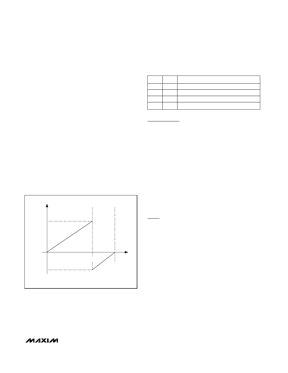
For proper operation, the driver has to meet the follow-
ing conditions: less than 25
Ω output impedance and
greater than 20mA peak output current capability.
Figure 6 shows a graph of typical input current versus
input voltage.
Output Load Requirements
The MAX13013–MAX13017/MAX3023–MAX3028 I/O are
designed to drive CMOS inputs. Do not load the I/O lines
with a resistive load less than 25k
Ω. Also, do not place an
RC circuit at the input of these devices to slow down the
edges. If a slower rise/fall time is required, refer to the
MAX3000E/MAX3001E logic-level-translators data sheet.
For I
2
C™ level translation, refer to the MAX3372E-
MAX3379E/MAX3390E–MAX3393E data sheet.
Enable Inputs
The MAX13013 single-, the MAX13014–MAX13017 dual-
and the MAX3023–MAX3028 (UCSP package) quad-level
translators feature an EN input. The MAX3023–MAX3028
(TSSOP package) quad-level translators feature both EN
and EN inputs (see Table 2 for operating mode). Note
that the MAX3023–MAX3028 (TSSOP package) have
internal pullup and pulldown circuitry on EN and EN,
respectively. If left unconnected, EN is pulled up to V
L
and EN is pulled down to GND.
Applications Information
Power-Supply Decoupling
To reduce ripple and the chance of introducing data
errors, bypass V
L
and V
CC
to ground with a 0.1µF
ceramic capacitor. Place all capacitors as close to the
power-supply inputs as possible.
Unidirectional vs. Bidirectional Level
Translator
The MAX13013/MAX13014/MAX3023 bidirectional
translators can operate as a unidirectional device to
translate signals without inversion. The MAX13015/
MAX13016/MAX13017/MAX3024–MAX3028 unidirec-
tional level translators, level shift data in one direction
(V
L
→ V
CC
or V
CC
→V
L
) on any single data line (see the
Ordering Information). These devices provide the
smallest solution (UCSP package) for unidirectional
level translation without inversion.
UCSP Applications Information
For the latest application details on UCSP construction,
dimensions, tape carrier information, PC board tech-
niques, bump-pad layout, and recommended reflow tem-
perature profiles, as well as the latest information on
reliability testing results, go to Maxim’s web site at
www.maxim-ic.com/ucsp to find the Application Note:
UCSP—A Wafer-Level Chip-Scale Package.
Table
2. MAX3023–MAX3028 (TSSOP
Package) Operating Mode
EN
EN
O PER A T IN G M OD E
0
0
Both I/O V
L
_ and I/O V
CC
_ are in tri-state.
V
L
0
Normal operation.
0
V
L
Both I/O V
L
_ and I/O V
CC
_ are in tri-state.
V
L
V
L
Both I/O V
L
_ and I/O V
CC
_ are in tri-state.
V
IN
V
TH_IN
/ R
IN
*
-(V
S
- V
TH_IN
) /
R
IN
*
I
IN
V
S
WHERE V
S
= V
CC
OR V
L
*R
IN
= 4k
Ω WHEN DRIVING V
L
SIDE; R
IN
= 150
Ω WHEN DRIVING V
CC
SIDE.
0
V
TH_IN
I
2
C is a trademark of Philips Corp.
Purchase of I
2
C components from Maxim Integrated Products, Inc. or one of its sublicensed Associated Companies, conveys a license
under the Philips I
2
C Patent Rights to use these components in an I
2
C system, provided that the system conforms to the I
2
C Standard
Specification as defined by Philips.
Figure 6. Typical I
IN
vs. V
IN