Rainbow Electronics MAX9820 User Manual
Page 2
MAX9820
DirectDrive Headphone Amplifier
with External Gain
2
_______________________________________________________________________________________
ABSOLUTE MAXIMUM RATINGS
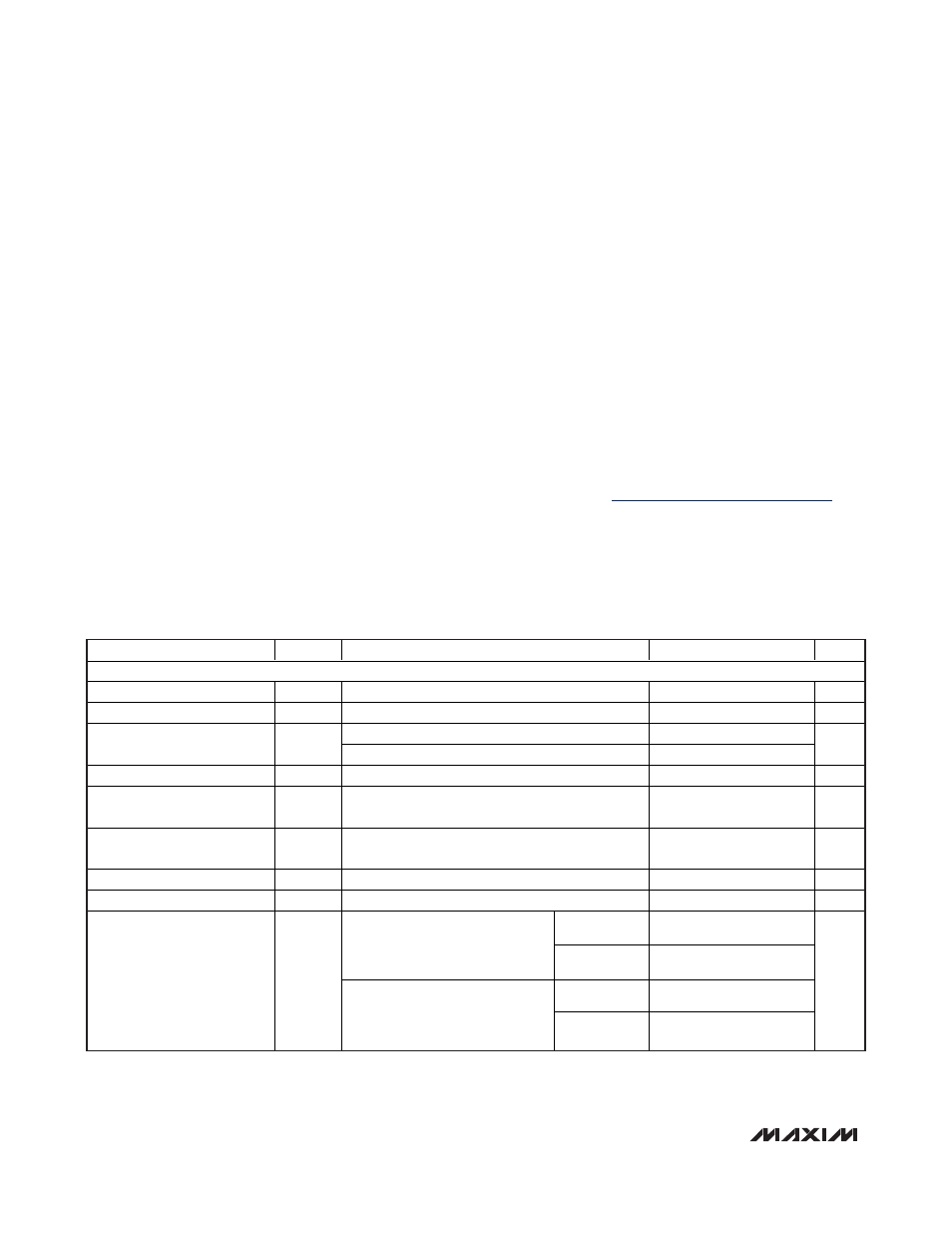
ELECTRICAL CHARACTERISTICS
(V
DD
= V
SHDN
= 5V, V
GND
= 0V, R
IN
= R
FB
= 40.2k
Ω (gain = -1V/V), C1 = C2 = 1µF, C3 = 10µF, R
LOAD
=
∞, T
A
= -40°C to +85°C,
unless otherwise noted. Typical values are at T
A
= +25°C, unless otherwise noted.) (Note 2)
Stresses beyond those listed under “Absolute Maximum Ratings” may cause permanent damage to the device. These are stress ratings only, and functional
operation of the device at these or any other conditions beyond those indicated in the operational sections of the specifications is not implied. Exposure to
absolute maximum rating conditions for extended periods may affect device reliability.
V
DD
to GND ..............................................................-0.3V to +6V
C1P to GND................................................-0.3V to (V
DD
+ 0.3V)
C1N to GND ................................................(V
SS
- 0.3V) to +0.3V
V
SS
to GND...............................................................-6V to +0.3V
OUTR, OUTL to GND.............................................................±3V
SHDN to GND...........................................................-0.3V to +6V
INR, INL to GND .........................................-0.3V to (V
DD
+ 0.3V)
OUTR, OUTL Short Circuit to GND, V
DD
....................Continuous
Short Circuit Between OUTL and OUTR ....................Continuous
Continuous Input Current (Into All Other Pins) .................±20mA
Continuous Power Dissipation (T
A
= +70°C)
10-Pin TDFN Single-Layer PCB (derate 18.5mW/°C
above +70°C)........................................................1481.5mW
Junction-to-Case Thermal Resistance (
θ
JC
) (Note 1)
10-Pin TDFN ................................................................8.5°C/W
Junction-to-Ambient Thermal Resistance (
θ
JA
) (Note 1)
10-Pin TDFN ...............................................................41.0°C/W
Continuous Power Dissipation (T
A
= +70°C)
10-Pin TDFN Multilayer PCB (derate 24.4mW/°C
above +70°C)...........................................................1951mW
Junction-to-Case Thermal Resistance (
θ
JC
) (Note 1)
10-Pin TDFN .................................................................9.0°C/W
Junction-to-Ambient Thermal Resistance (
θ
JA
) (Note 1)
10-Pin TDFN ...............................................................41.0°C/W
Operating Temperature Range ...........................-40°C to +85°C
Storage Temperature Range .............................-65°C to +150°C
Junction Temperature ......................................................+150°C
Lead Temperature (soldering, 10s) .................................+300°C
PARAMETER
SYMBOL
CONDITIONS
MIN
TYP
MAX
UNITS
GENERAL
Supply Voltage Range
V
DD
Guaranteed by PSRR test
2.7
5.5
V
Undervoltage Lockout
UVLO
2.2
V
V
DD
= 3.3V
3.0
4.6
Quiescent Current
I
DD
V
DD
= 5V
4.0
6.0
mA
Shutdown Current
I
SHDN
V
SHDN
= 0V, T
A
= +25°C
< 0.1
1
µA
Output Signal Attenuation in
Shutdown
V
SHDN
= 0V, V
IN
= 1V
RMS
, R
LOAD
= 10k
Ω
-110
dBV
Output Impedance in
Shutdown
V
SHDN
= 0V
0.6
k
Ω
Turn-On Time
t
ON
0.56
ms
Output Offset Voltage
V
OS
T
A
= +25°C (Note 3)
±0.1
±0.5
mV
Into shutdown
-79
Z
LOAD
= 32
Ω + 1µH, peak
voltage, A-weighted, 32 samples
per second (Notes 3, 4)
Out of
shutdown
-77
Into shutdown
-62
Click-and-Pop Level
K
CP
Z
LOAD
= 10k
Ω, peak voltage,
A-weighted, 32 samples per
second (Notes 3, 4)
Out of
shutdown
-58
dBV
Note 1: Package thermal resistances were obtained using the method described in JEDEC specification JESD51-7, using a four-
layer board. For detailed information on package thermal considerations, refer to
www.maxim-ic.com/thermal-tutorial
.