Chip information, Functional diagram/typical operating circuit, Amplifier gain – Rainbow Electronics MAX9820 User Manual
Page 11: Layout and grounding
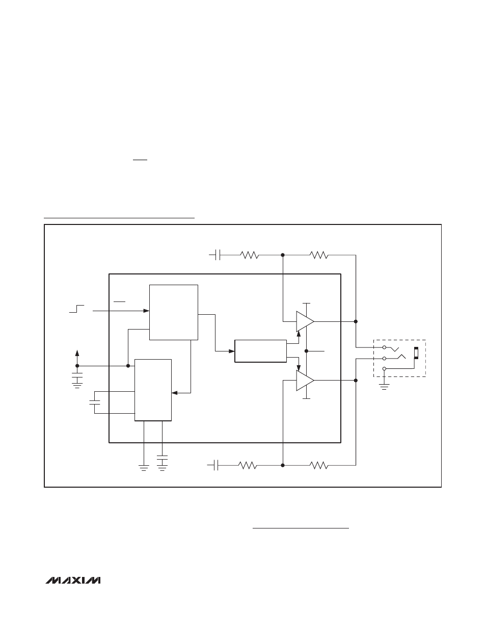
Amplifier Gain
The gain of the MAX9820 is set externally using input
and feedback resistors (see the
Functional Diagram/
Typical Operating Circuit
). The gain is:
Choose feedback resistor values in the tens of k
Ω
range.
Layout and Grounding
Proper layout and grounding are essential for optimum
performance. Connect EP and GND together at a single
point on the PCB. Ensure ground return resistance is
minimized for optimum crosstalk performance. Place
the power-supply bypass capacitor, the charge-pump
hold capacitor, and the charge-pump flying capacitor
as close as possible to the MAX9820. Route all traces
that carry switching transients away from the audio sig-
nal path.
A
R
R
V V
V
FB
IN
= −
( / )
MAX9820
DirectDrive Headphone Amplifier
with External Gain
______________________________________________________________________________________
11
Chip Information
PROCESS: BiCMOS
CHARGE
PUMP
CLICK-AND-POP
SUPPRESSION
C
IN
1.0
µF
R
IN
40.2k
Ω
R
FB
40.2k
Ω
INR
INL
SHDN
GND
TO V
DD
TO V
DD
TO V
SS
OUTL
OUTR
UVLO/SHUTDOWN
CONTROL
C1P
C1N
2.7V TO 5.5V
C3
10
µF
C2
1.0
µF
C1
1.0
µF
V
DD
V
SS
OFF
ON
1
2
8
10
9
3
6
7
4
5
HEADPHONE
JACK
C
IN
1.0
µF
R
IN
40.2k
Ω
R
FB
40.2k
Ω
-1
-1
Functional Diagram/Typical Operating Circuit