Ac electrical characteristics, Dc electrical characteristics – Rainbow Electronics ADC08161 User Manual
Page 4
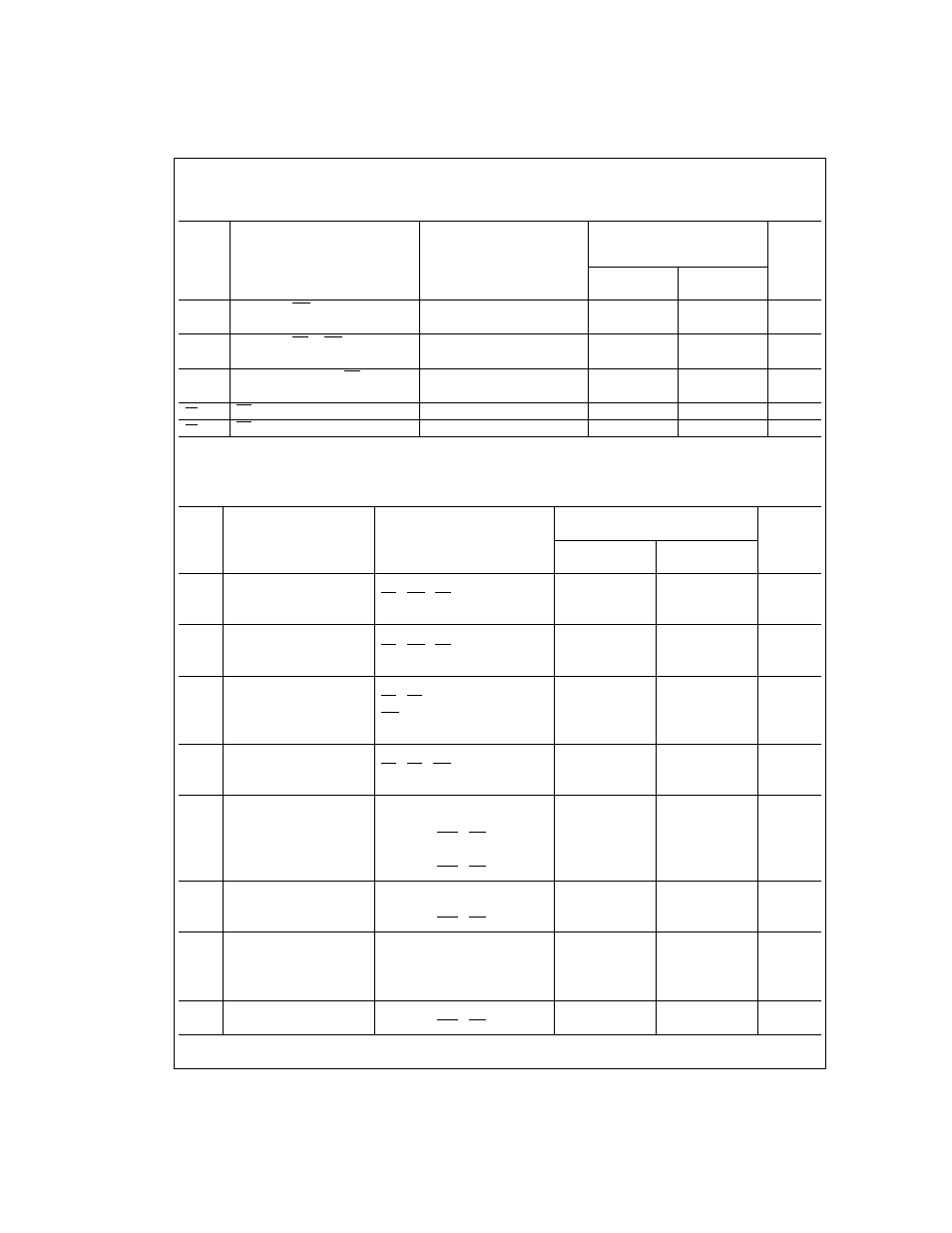
AC Electrical Characteristics
(Continued)
The following specifications apply for V
+
= 5V, t
r
= t
f
= 10 ns, V
REF+
= 5V, V
REF−
= 0V unless otherwise specified. Boldface
limits apply for T
A
= T
J
= T
MIN
to T
MAX
; all other limits T
A
= T
J
= 25˚C.
Symbol
Parameter
Conditions
ADC08161BIN, ADC08161CIN,
Units
(Limit)
ADC08161BIWM,
ADC08161CIWM
Typical
Limit
(Note 7)
(Note 8)
t
ID
Delay from INT
R
L
= 3 k
Ω
, C
L
= 100 pF
0
15
ns (max)
to Output Valid
(
Figure 4
)
t
RI
Delay from RD to INT
Mode Pin = V
+
, t
RD
≤
t
INTL
60
115
ns (max)
(
Figure 2
)
t
N
Time between End of RD
(
Figures 1, 2, 3, 4, 5
)
50
50
ns (min)
and Start of New Conversion
t
CSS
CS Setup Time
(
Figures 1, 2, 3, 4, 5
)
0
0
ns (max)
t
CSH
CS Hold Time
(
Figures 1, 2, 3, 4, 5
)
0
0
ns (max)
DC Electrical Characteristics
The following specifications apply for V
+
= 5V unless otherwise specified. Boldface limits apply for T
A
= T
J
= T
MIN
to T
MAX
;
all other limits T
A
= T
J
= 25˚C.
Symbol
Parameter
Conditions
ADC08161BIN, ADC08161CIN,
Units
(Limit)
ADC08161BIWM, ADC08161CIWM
Typical
Limit
(Note 7)
(Note 8)
V
IH
Logic “1” Input Voltage
V
+
= 5.5 V
CS , WR , RD , A0, A1, A2 Pins
2.0
V (min)
Mode Pin
3.5
V
IL
Logic “0” Input Voltage
V
+
= 4.5V
CS , WR , RD , A0, A1, A2 Pins
0.8
V (max)
Mode Pin
1.5
I
IH
Logic “1” Input Current
V
H
= 5V
CS , RD , A0, A1, A2 Pins
0.005
1
WR Pin
0.1
3
µA (max)
Mode Pin
50
200
I
IL
Logic “0” Input Current
V
L
= 0V
CS , RD , WR , A0, A1, A2
Mode Pins
−0.005
−2
µA (max)
V
OH
Logic “1” Output Voltage
V
+
= 4.75V
I
OUT
= −360 µA
2.4
V (min)
DB0–DB7, OFL , INT
I
OUT
= −10 µA
4.5
V (min)
DB0–DB7, OFL , INT
V
OL
Logic “0” Output Voltage
V
+
= 4.75V
I
OUT
= 1.6 mA
0.4
V (max)
DB0–DB7, OFL , INT , RDY
I
O
TRI-STATE Output Current
V
OUT
= 5.0V
0.1
3
µA (max)
DB0–DB7, RDY
V
OUT
= 0V
−0.1
−3
µA (max)
DB0–DB7, RDY
I
SOURCE
Output Source Current
V
OUT
= 0V
−26
−6
mA (min)
DB0–DB7, OFL , INT
www.national.com
4