Application information – Rainbow Electronics ADC08161 User Manual
Page 13
Application Information
(Continued)
The voltage at V
REF−
sets the input level that produces a
digital output of all zeroes. Through V
IN
is not itself differen-
tial, the reference design affords nearly differential-input ca-
pability for some measurement applications.
Figure 7
shows
one possible differential configuration.
It should be noted that, while the two V
REF
inputs are fully
differential, the digital output will be zero for any analog input
voltage if V
REF−
≥
V
REF+
.
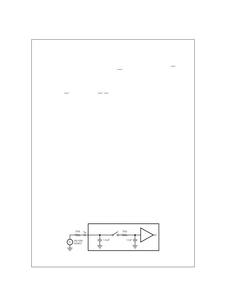
4.0 ANALOG INPUT AND SOURCE IMPEDANCE
The ADC08161’s analog input circuitry includes an analog
switch with an “on” resistance of 70
Ω
and a 1.4 pF capacitor
(
Figure 7
). The switch is closed during the A/D’s input signal
acquisition time (while WR is low when using the WR -RD
Mode). A small transient current flows into the input pin each
time the switch closes. A transient voltage, whose magnitude
can increase as the source impedance increases, may be
present at the input. So long as the source impedance is less
than 500
Ω
, the input voltage transient will not cause errors
and need not be filtered.
Large source impedances can slow the charging of the sam-
pling capacitors and degrade conversion accuracy. There-
fore, only signal sources with output impedances less than
500
Ω
should be used if rated accuracy is to be achieved at
the minimum sample time (100 ns maximum). A signal
source with a high output impedance should have its output
buffered with an operational amplifier. Any ringing or voltage
shifts at the op amp’s output during the sampling period can
result in conversion errors.
Some suggested input configurations using the internal 2.5V
reference, an external reference, and adjusting the input
span are shown in
Figure 8
.
Correct conversion results will be obtained for input voltages
greater than GND − 100 mV and less than V
+
+ 100 mV. Do
not allow the signal source to drive the analog input pin more
than 300 mV higher than V
+
, or more than 300 mV lower
than GND. The current flowing through any analog input pin
should be limited to 5 mA or less to avoid permanent dam-
age to the IC if an analog input pin is forced beyond these
voltages. The sum of all the overdrive currents into all pins
must be less than 20 mA. Some sort of protection scheme
should be used when the input signal is expected to extend
more than 300 mV beyond the power supply limits. A simple
protection network using resistors and diodes is shown in
Figure 9
.
5.0 INHERENT SAMPLE-AND-HOLD
An important benefit of the ADC08161’s input architecture is
the inherent sample-and-hold (S/H) and its ability to mea-
sure relatively high speed signals without the help of an ex-
ternal S/H. In a non-sampling converter, regardless of its
speed, the input must remain stable to at least
1
⁄
2
LSB
throughout the conversion process if full accuracy is to be
maintained. Consequently, for many high speed signals, this
signal must be externally sampled and held stationary during
the conversion.
The ADC08161 is suitable for DSP-based systems because
of the direct control of the S/H through the WR signal. The
WR input signal allows the A/D to be synchronized to a DSP
system’s sampling rate or to other ADC08161s.
The ADC08161 can perform accurate conversions of
full-scale input signals at frequencies from DC to more than
300 kHz (full power bandwidth) without the need of an exter-
nal sample-and-hold (S/H).
6.0 INTERNAL BANDGAP REFERENCE
The ADC08161 has an internal bandgap 2.5V reference that
can be used as the V
REF+
input. A parallel combination of a
0.1 µF ceramic capacitor and a 220 µF tantalum capacitor
should be used to bypass the V
REFOUT
pin. This reduces
possible noise pickup that could cause conversion errors.
7.0 LAYOUT, GROUNDS, AND BYPASSING
In order to ensure fast, accurate conversions from the
ADC08161, it is necessary to use appropriate circuit board
layout techniques. Ideally, the analog-to-digital converter’s
ground reference should be low impedance and free of noise
from other parts of the system. Digital circuits can produce a
great deal of noise on their ground returns and, therefore,
should have their own separate ground lines. Best perfor-
mance is obtained using separate ground planes should be
provided for the digital and analog parts of the system.
The analog inputs should be isolated from noisy signal
traces to avoid having spurious signals couple to the input.
Any external component (e.g., an input filter capacitor) con-
nected across the inputs should be returned to a very clean
ground point. Incorrectly grounding the ADC08161 may re-
sult in reduced conversion accuracy.
The V
+
supply pin, V
REF+
, and V
REF−
(if not grounded)
should be bypassed with a parallel combination of a 0.1 µF
ceramic capacitor and a 10 µF tantalum capacitor placed as
close as possible to the pins using short circuit board traces.
See
Figures 8, 9
.
DS011149-18
FIGURE 7. ADC08161 Equivalent Input Circuit Model
13
www.national.com