Converter characteristics, Ac electrical characteristics – Rainbow Electronics ADC08161 User Manual
Page 3
Converter Characteristics
(Continued)
The following specifications apply for RD Mode, V
+
= 5V, V
REF+
= 5V, and V
REF−
= GND unless otherwise specified. Bold-
face limits apply for T
A
= T
J
= T
MIN
to T
MAX
; all other limits T
A
= T
J
= 25˚C.
Symbol
Parameter
Conditions
Typical
Limits
Units
(Note 7)
(Note 8)
(Limit)
THD
Total Harmonic Distortion
V
IN
= 4.85 V
p-p
0.5
%
f
IN
= 20 Hz to 20 kHz
S/N
Signal-to-Noise Ratio
V
IN
= 4.85 V
p-p
50
dB
f
IN
= 20 Hz to 20 kHz
IMD
Intermodulation Distortion
V
IN
= 4.85 V
p-p
50
dB
f
IN
= 20 Hz to 20 kHz
C
VIN
Analog Input Capacitance
25
pF
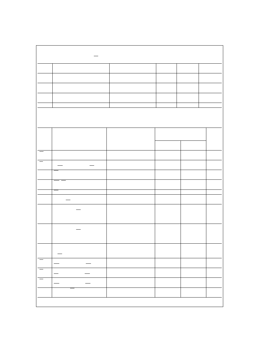
AC Electrical Characteristics
The following specifications apply for V
+
= 5V, t
r
= t
f
= 10 ns, V
REF+
= 5V, V
REF−
= 0V unless otherwise specified. Boldface
limits apply for T
A
= T
J
= T
MIN
to T
MAX
; all other limits T
A
= T
J
= 25˚C.
Symbol
Parameter
Conditions
ADC08161BIN, ADC08161CIN,
Units
(Limit)
ADC08161BIWM,
ADC08161CIWM
Typical
Limit
(Note 7)
(Note 8)
t
WR
Write Time
Mode Pin to V
+
100
100
ns (min)
(
Figures 2, 3, 4
)
t
RD
Read Time (Time from Rising Edge
Mode Pin to V
+
, (
Figure 2
)
350
350
ns (min)
of WR to Falling Edge of RD )
t
RDW
RD Width
Mode Pin to GND (
Figure 5
)
200
250
ns (min)
400
400
ns (max)
t
CONV
WR -RD Mode Conversion Time
Mode Pin to V
+
, (
Figure 2
)
500
560
ns (max)
(t
WR
+ t
RD
+ t
ACC1
)
t
CRD
RD Mode Conversion Time
Mode Pin to GND, (
Figure 1
)
655
900
ns (max)
t
ACCO
Access Time (Delay from Falling
C
L
≤
100 pF, Mode Pin to GND
640
900
ns (max)
Edge of RD to Output Valid)
(
Figure 1
)
t
ACC1
Access Time (Delay from
C
L
≤
10 pF
45
ns
Falling Edge of RD
C
L
= 100 pF
50
110
ns (max)
to Output Valid)
Mode Pin to V
+
, t
RD
≤
t
INTL
(
Figure 2
)
t
ACC2
Access Time (Delay from
C
L
≤
10 pF
25
ns
Falling Edge of RD
C
L
= 100 pF
30
55
ns (max)
to Output Valid)
t
RD
>
t
INTL
,
(
Figures 3, 5
)
t
1H
, t
0H
TRI-STATE
®
Control
R
L
= 3 k
Ω
, C
L
= 10 pF
(Delay from Rising Edge
(
Figures 1, 2, 3, 4, 5
)
30
60
ns (max)
of RD to HI-Z State)
t
INTL
Delay from Rising Edge of
Mode Pin = V
+
, C
L
= 50 pF
520
690
ns (max)
WR to Falling Edge of INT
(
Figures 3, 4
)
t
INTH
Delay from Rising Edge of
C
L
= 50 pF,
50
95
ns (max)
RD to Rising Edge of INT
(
Figures 1, 2, 3, 5
)
t
INTH
Delay from Rising Edge of
C
L
= 50 pF, (
Figure 4
)
45
95
ns (max)
WR to Rising Edge of INT
t
RDY
Delay from CS to RDY
Mode Pin = 0V, C
L
= 50 pF,
25
45
ns (max)
R
L
= 3 k
Ω
, (
Figure 1
)
3
www.national.com