Max7457, Video switch for dual scart connectors, Applications information – Rainbow Electronics MAX7457 User Manual
Page 6: Chip information, Pin configuration, Table 1. output clamp level
MAX7457
Output Buffers
Each output buffer has a fixed gain of +6dB and can
drive two 150
Ω video loads with a 2V
P-P
signal. The
MAX7457 can drive an AC-coupled load or drive a DC-
coupled load, eliminating the large coupling capaci-
tors. The output buffers drive DC loads with an output
blanking level of less than 1V.
Output Clamp Level
The video signal processed by channel INA_ (CVBS
video signal) must include a sync pulse. This sync
pulse provides the required timing to all four channels.
When channel INA_ detects a sync pulse, the DC
restore loop is activated. The function of the loop is to
set the DC level of the video signal to a specified volt-
age. See
Table 1 for clamp levels.
Input Multiplexer
The MAX7457 has a 2-to-1 input multiplexer at channel
INA_. The input to the CVBS channel comes from
either a DAC output or from a CVBS source and is
selected by SELA. Pull SELA low to select INA1 or high
to select INA2.
Applications Information
Input Considerations
Use 0.1µF ceramic capacitors to AC-couple the inputs.
The input capacitors store a DC level so the outputs are
clamped to an appropriate DC voltage level.
Output Considerations
The outputs are typically connected to a 75
Ω series
back-match resistor followed by the video cable.
Because of the inherent divide-by-two of this configura-
tion, the voltage on the video cable is always less than
1V, complying with industry-standard video require-
ments such as the European SCART standard (which
allows up to 2V of DC on the video cable). The video
buffer can also drive an AC-coupled video load. An
output capacitor as low as 220µF provides good
video performance.
Power-Supply Bypassing and Layout
The MAX7457 operates from a single +5V supply.
Bypass V
CC
to GND with a 0.1µF capacitor. Place all
external components as close to the device as possible.
Exposed Pad
The TQFN package has an exposed pad on the bottom
of the package. This pad is electrically connected to
GND and should be connected to the ground plane for
improved thermal conductivity. Do not route signals
under this package.
Video Switch for Dual SCART Connectors
6
_______________________________________________________________________________________
Chip Information
TRANSISTOR COUNT: 4579
PROCESS: BiCMOS
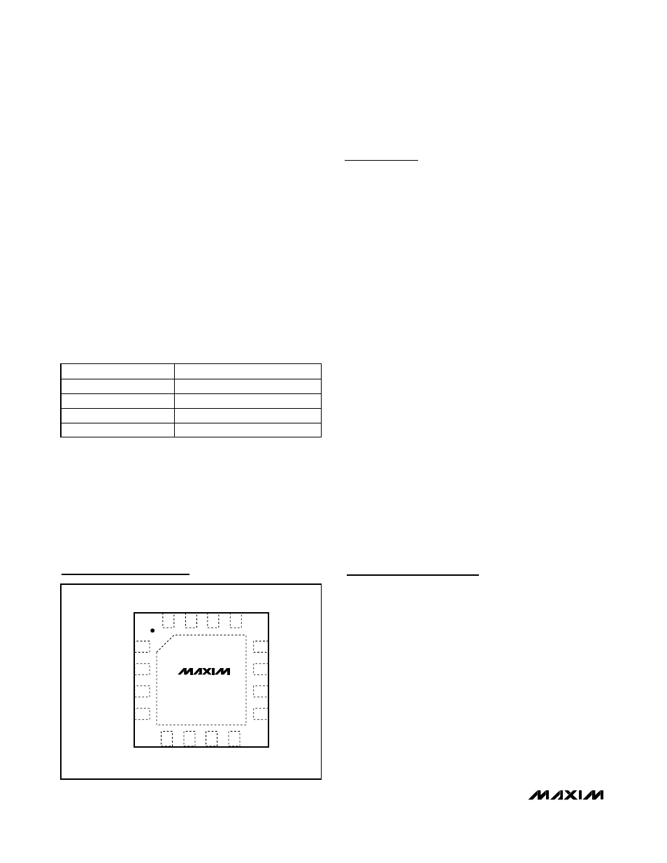
Pin Configuration
Table 1. Output Clamp Level
CHANNEL
CLAMP LEVEL (V)
A
0.9
B
1.5
C
1.5
D
1.5
16
1
2
3
4
12
11
10
9
15
14
13
5
6
7
8
INA1
INA2
N.C.
OUT
A
OUTB
OUTC
OUTD
V
CC
INC
IND
DISABLE
SELA
N.C.
GND
N.C.
INB
TOP VIEW
MAX7457
TQFN