Max7457 video switch for dual scart connectors – Rainbow Electronics MAX7457 User Manual
Page 2
MAX7457
Video Switch for Dual SCART Connectors
2
_______________________________________________________________________________________
ABSOLUTE MAXIMUM RATINGS
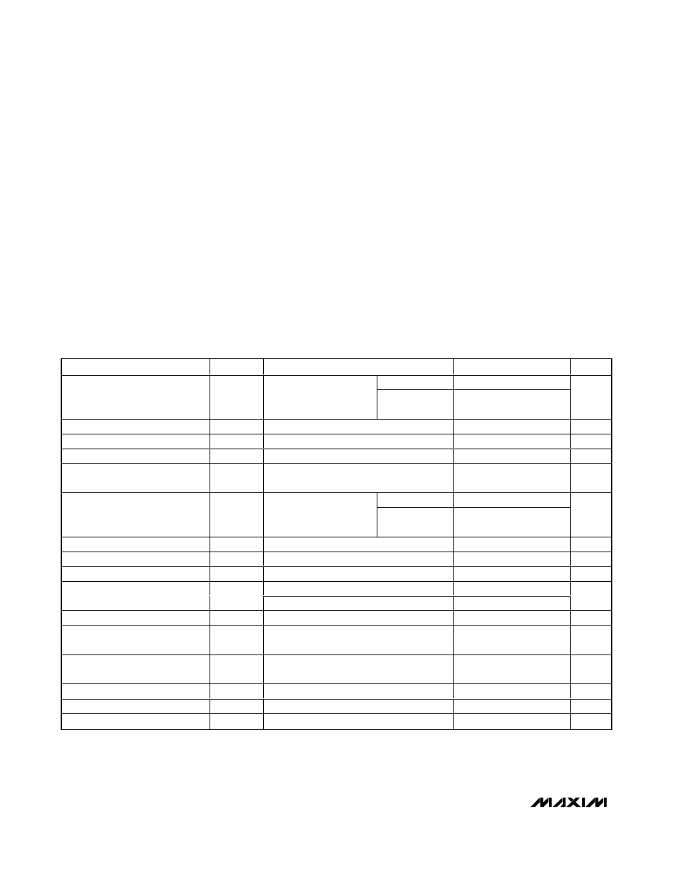
ELECTRICAL CHARACTERISTICS
(V
CC
= +5V ±5%, C
L
= 0 to 20pF, R
L
= 75
Ω to GND for DC-coupled load, R
L
= 75
Ω to V
CC
/2 for AC-coupled load, T
A
= T
MIN
to
T
MAX
, unless otherwise noted. Typical values are at V
CC
= 5V, T
A
= +25°C.)
Stresses beyond those listed under “Absolute Maximum Ratings” may cause permanent damage to the device. These are stress ratings only, and functional
operation of the device at these or any other conditions beyond those indicated in the operational sections of the specifications is not implied. Exposure to
absolute maximum rating conditions for extended periods may affect device reliability.
V
CC
to GND ..............................................................-0.3V to +6V
INA1, INA2, INB, INC, IND to GND ............-0.3V to (V
CC
+ 0.3V)
OUTA, OUTB, OUTC, OUTD to GND .........-0.3V to (V
CC
+ 0.3V)
SELA, DISABLE to GND .............................-0.3V to (V
CC
+ 0.3V)
Maximum Current into Any Pin Except V
CC
and GND .....±50mA
Continuous Power Dissipation (T
A
= +70°C)
16-Pin TQFN (derate 20.8mW/°C
above +70°C)..........................................................1666.7mW
Operating Temperature Range ...........................-40°C to +85°C
Storage Temperature Range .............................-65°C to +150°C
Junction Temperature ......................................................+150°C
Lead Temperature (soldering, 10s) .................................+300°C
PARAMETER
SYMBOL
CONDITIONS
MIN
TYP
MAX
UNITS
Channel INA_
+0.9
+1.2
+1.5
Passband Flatness
f = 100kHz to 5MHz,
relative to 100kHz
Channels INB,
INC, IND
-0.75
+0.15
+0.75
dB
Stopband Attenuation
A
SB
f
≥ 27MHz
40
43
dB
Differential Gain
dG
5-step modulated staircase
0.15
0.5
%
Differential Phase
d
θ
5-step modulated staircase
0.15
0.5
Degrees
Signal-to-Noise Ratio
SNR
Peak signal (2V
P-P
) to RMS noise, f = 100Hz
to 50MHz
80
dB
Channel INA_
17
30
Group Delay Deviation
∆t
g
Deviation from
100kHz to 4.1MHz
Channels INB,
INC, IND
11
20
ns
Line-Time Distortion
H
DIST
18µs, 100 IRE bar
0.3
%
Field-Time Distortion
V
DIST
130 lines, 18µs, 100 IRE bar
0.5
%
Clamp Settling Time
t
CLAMP
To ±1%
300
Lines
Channel INA_
0.6
0.9
1.1
Output DC Clamp Level
Channel INB, INC, IND
1.1
1.5
1.8
V
Low-Frequency Gain Accuracy
A
V
f = 100kHz, relative to gain of +6dB
-3
+3
%
Low-Frequency Gain Matching
A
V(MATCH)
Low-frequency channel-to-channel
matching, f = 100kHz
4
%
Group Delay Matching
t
g(MATCH)
Low-frequency channel-to-channel
matching, f = 100kHz
2
ns
Channel-to-Channel Crosstalk
X
TALK
f = 100kHz to 3.58MHz
-60
dB
Disabled Output Impedance
Z
DISABLE
At 5MHz
2
k
Ω
Output Short-Circuit Current
I
SC
OUT_ shorted to GND or V
CC
70
mA