Detailed description, Typical application circuit, Controller function – Rainbow Electronics MAX15051 User Manual
Page 9
MAX15050/MAX15051
C9
0.1
µF
OPTIONAL
C1
22
µF
OUTPUT
1.8V/4A
INPUT
2.9V TO 5.5V
C3
0.1
µF
BST
LX
IN
V
DD
FB
COMP
C12
56pF
C10
1000pF
C11
1500pF
R4
5.62k
Ω
R5
20k
Ω
PWRGD
L1
0.82
µH
C8
0.033
µF
C2
47
µF
R6
71.5
Ω
C4
0.01
µF
C5
2.2
µF
REFIN/SS
GND
V
DD
MAX15050
MAX15051
U1
IN
EN
ON
OFF
BST
LX
LX
R10
2.2
Ω
C15
1000pF
GND
R3
8.06k
Ω
1%
R7
4.02k
Ω
1%
High-Efficiency, 4A, 1MHz, Step-Down Regulators
with Integrated Switches in 2mm x 2mm Package
_______________________________________________________________________________________
9
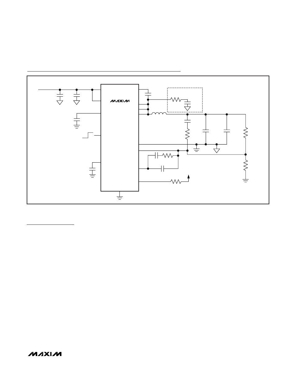
Figure 1. All-Ceramic Capacitor Design with V
OUT
= 1.8V
Detailed Description
The MAX15050/MAX15051 high-efficiency, voltage-
mode switching regulators can deliver up to 4A of out-
put current. The MAX15050/MAX15051 provide output
voltages from 0.6V to (0.9 x V
IN
) from 2.9V to 5.5V input
supplies, making them ideal for on-board point-of-load
applications. The output-voltage accuracy is better than
±1% over load, line, and temperature.
The MAX15050/MAX15051 feature a 1MHz fixed switch-
ing frequency, allowing the user to achieve all-ceramic
capacitor designs and fast transient responses. The high
operating frequency minimizes the size of external com-
ponents. The MAX15050/MAX15051 are available in a
2mm x 2mm, 16-bump (4 x 4 array), 0.5mm pitch WLP
package. The REFIN/SS function makes the
MAX15050/MAX15051 ideal solutions for DDR and track-
ing power supplies. Using internal low-R
DS(ON)
(24m
Ω
and 18m
Ω) n-channel MOSFETs for the high- and low-
side switches, respectively, maintains high efficiency at
both heavy-load and high-switching frequencies.
The MAX15050/MAX15051 employ voltage-mode con-
trol architecture with a high-bandwidth (> 26MHz) error
amplifier. The op-amp voltage-error amplifier works with
type III compensation to fully utilize the bandwidth of
the high-frequency switching to obtain fast transient
response. Adjustable soft-start time provides flexibilities
to minimize input startup inrush current. An open-drain,
power-good (PWRGD) output goes high impedance
when V
FB
exceeds 92.5% of V
REFIN/SS
and V
REFIN/SS
is above 0.54V. PWRGD goes low when V
FB
falls below
90% of V
REFIN/SS
or V
REFIN/SS
is below 0.54V.
Controller Function
The controller logic block is the central processor that
determines the duty cycle of the high-side MOSFET
under different line, load, and temperature conditions.
Under normal operation, where the current-limit and
temperature protection are not triggered, the controller
logic block takes the output from the PWM comparator
and generates the driver signals for both high-side and
low-side MOSFETs. The control logic block controls the
break-before-make logic and the timing for charging
the bootstrap capacitors. The error signal from the volt-
age-error amplifier is compared with the ramp signal
generated by the oscillator at the PWM comparator to
produce the required PWM signal. The high-side switch
turns on at the beginning of the oscillator cycle and
Typical Application Circuit