Rainbow Electronics MAX15051 User Manual
Page 13
MAX15050/MAX15051
The above equations are based on the assumptions that
C1 >> C2, and R3 >> R2, which are true in most appli-
cations. Placements of these poles and zeros are deter-
mined by the frequencies of the double pole and ESR
zero of the power transfer function. It is also a function
of the desired closed-loop bandwidth. The following
section outlines the step-by-step design procedure to
calculate the required compensation components for
the MAX15050/MAX15051.
The output voltage is determined by:
where V
FB
is the feedback voltage equal to V
REFIN/SS
or 0.6V depending whether or not an external reference
voltage is applied to REFIN/SS.
For V
OUT
= V
FB
, R4 is not needed.
The zero-cross frequency of the closed-loop, f
C
, should
be between 10% and 20% of the switching frequency,
f
S
(1MHz). A higher zero-cross frequency results in
faster transient response. Once f
C
is chosen, C1 is cal-
culated from the following equation:
where V
P-P
= 1V
P-P
(typ).
Due to the underdamped nature of the output LC double
pole, set the two zero frequencies of the type III compen-
sation less than the LC double-pole frequency to provide
adequate phase boost. Set the two zero frequencies to
80% of the LC double-pole frequency. Hence:
Setting the second compensation pole, f
P2_EA
, at
f
Z_ESR
yields:
Set the third compensation pole at 1/2 of the switching
frequency (500kHz) to gain phase margin. Calculate
C2 as follows:
The above equations provide accurate compensation
when the zero-cross frequency is significantly higher
than the double-pole frequency. When the zero-cross
frequency is near the double-pole frequency, the actual
zero-cross frequency is higher than the calculated fre-
quency. In this case, lowering the value of R1 reduces
the zero-cross frequency. Also, set the third pole of the
type III compensation close to the switching frequency
(1MHz) if the zero-cross frequency is above 200kHz to
boost the phase margin. The recommended range for
R3 is 2k
Ω to 10kΩ. Note that the loop compensation
remains unchanged if only R4’s resistance is altered to
set different outputs.
C
x R x f
S
2
1
1
=
π
R
C
x ESR
C
O
2
3
=
C
x R
x
L x C
x R
ESR
R
R
O
O
L
O
3
1
0 8
3
=
+
+
.
(
)
R
x C
x
L x C
x R
ESR
R
R
O
O
L
O
1
1
0 8
1
=
+
+
.
(
)
C
V
V
x
x R x
R
R
f
IN
P P
L
O
C
1
1 5625
2
3
1
=
⎛
⎝⎜
⎞
⎠⎟
+
×
−
.
(
)
π
R
V
R
V
V
FB
OUT
FB
4
3
=
×
−
(
)
f
x
P
EA
3
1
2
_
=
π R
R x C
1
2
f
x R
x C
P
EA
1
2
2
3
2 _
=
π
High-Efficiency, 4A, 1MHz, Step-Down Regulators
with Integrated Switches in 2mm x 2mm Package
______________________________________________________________________________________
13
L
C
OUT
V
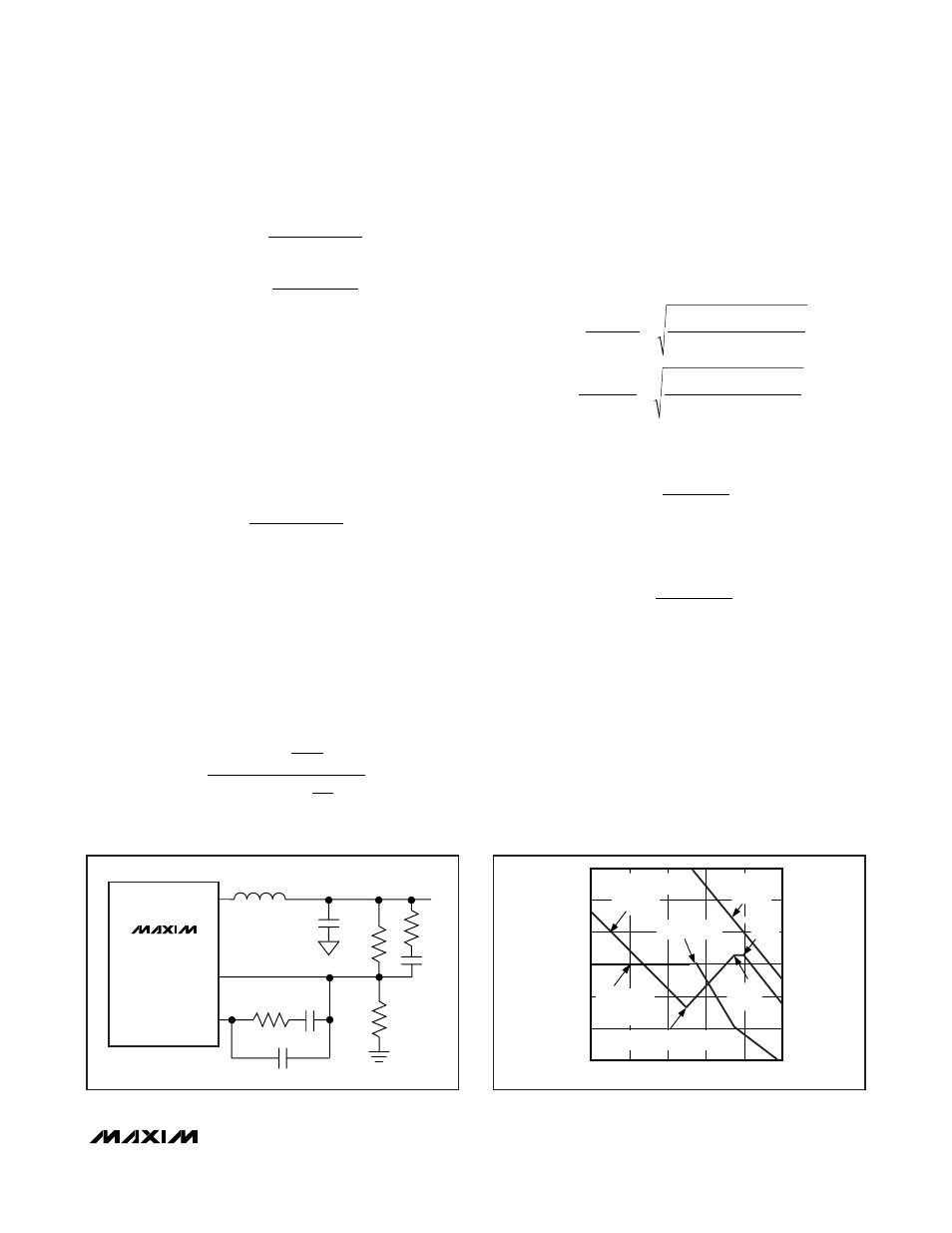
OUT
R3
R4
R1
COMP
FB
LX
C1
C3
R2
C2
MAX15050
MAX15051
Figure 4. Type III Compensation Network
DOUBLE POLE
GAIN (dB)
FREQUENCY (Hz)
SECOND
POLE
FIRST AND SECOND ZEROS
POWER-STAGE
TRANSFER
FUNCTION
COMPENSATION
TRANSFER
FUNCTION
OPEN-LOOP
GAIN
THIRD
POLE
Figure 5. Type III Compensation Illustration