Bias – Rainbow Electronics MAX4039 User Manual
Page 2
MAX4036–MAX4039
Low I
BIAS
, +1.4V/800nA, Rail-to-Rail Op Amps
with +1.2V Buffered Reference
2
_______________________________________________________________________________________
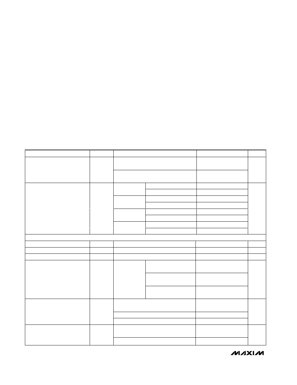
ABSOLUTE MAXIMUM RATINGS
ELECTRICAL CHARACTERISTICS
(V
DD
= +3V, V
SS
= V
CM
= 0V, V
OUT_
= V
DD
/2, R
L
to V
DD
/2, C
L
= 15pF,
T
A
= +25°C, unless otherwise specified.)
Stresses beyond those listed under “Absolute Maximum Ratings” may cause permanent damage to the device. These are stress ratings only, and functional
operation of the device at these or any other conditions beyond those indicated in the operational sections of the specifications is not implied. Exposure to
absolute maximum rating conditions for extended periods may affect device reliability.
V
DD
to V
SS
.............................................................-0.3V to +4.0V
INA+, INB+, INA-, INB-, IN+, IN-, OUTA,
OUTB, OUT, REF .........................(V
SS
- 0.3V) to (V
DD
+ 0.3V)
OUTA, OUTB, OUT, REF Shorted to V
SS
or V
DD
.......Continuous
Maximum Continuous Power Dissipation (T
A
= +70°C)
5-Pin SC70 (derate 3.1mW/°C above +70°C) ..............247mW
6-Pin SOT23 (derate 8.7mW/°C above +70°C)............696mW
8-Pin µMAX (derate 4.5mW/°C above +70°C) .............362mW
8-Pin TDFN (derate 24.4mW/°C above +70°C) .........1951mW
10-Pin µMAX (derate 5.6mW/°C above +70°C) ...........444mW
10-Pin TDFN (derate 24.4mW/°C above +70°C) .......1951mW
Operating Temperature Range ...........................-40°C to +85°C
Junction Temperature .....................................................+150°C
Storage Temperature Range .............................-65°C to +150°C
Lead Temperature (soldering, 10s) .................................+300°C
PARAMETER
SYMBOL
CONDITIONS
MIN
TYP
MAX
UNITS
MAX4036/MAX4038, guaranteed by PSRR
tests
1.4
3.6
Supply Voltage Range
V
DD
MAX4037/MAX4039, guaranteed by PSRR
and line regulation tests
1.8
3.6
V
V
DD
= 1.4V
0.8
1.2
MAX4036
V
DD
= 3.6V
0.9
1.3
V
DD
= 1.8V
1.9
2.4
MAX4037
V
DD
= 3.6V
2.0
2.5
V
DD
= 1.4V
1.7
2.3
MAX4038
V
DD
= 3.6V
1.9
2.5
V
DD
= 1.8V
2.8
4.0
Supply Current
I
DD
MAX4039
V
DD
= 3.6V
3.0
4.1
µA
OPERATIONAL AMPLIFIERS
Input Offset Voltage
V
OS
±0.2
±2.0
mV
Input Bias Current
I
B
(Note 1)
±1.0
±10
pA
Input Offset Current
I
OS
(Note 1)
±0.3
±20
pA
V
D D
= 1.4V
( M AX 4036/M AX 4038 onl y)
V
SS
V
DD
-
0.4
V
DD
= 1.8V
V
SS
V
DD
-
0.3
Input Common-Mode Voltage
Range
V
CM
Guaranteed by
CMRR test
V
DD
= 3.3V
V
SS
V
DD
-
0.2
V
V
DD
= 1.4V, V
SS
† V
CM
† (V
DD
- 0.4V)
(MAX4036/MAX4038 only)
50
70
V
DD
= 1.8V, V
SS
† V
CM
† (V
DD
- 0.3V)
50
70
Common-Mode Rejection Ratio
CMRR
V
DD
= 3.3V, V
SS
† V
CM
† (V
DD
- 0.2V)
56
76
dB
1.4V
† V
DD
† 3.6V (MAX4036/MAX4038
only)
62
82
Power-Supply Rejection Ratio
PSRR
1.8V
† V
DD
† 3.6V
62
84
dB