Bias, Chip information, Selector guide – Rainbow Electronics MAX4039 User Manual
Page 12
MAX4036–MAX4039
Low I
BIAS
, +1.4V/800nA, Rail-to-Rail Op Amps
with +1.2V Buffered Reference
12
______________________________________________________________________________________
3)
Calculate R1:
4)
Choose the threshold voltage for V
IN
rising (V
THR
).
In this example, choose V
THR
= 2.0V.
5)
Calculate R2:
6)
Verify the threshold voltages with these formulas:
V
IN
rising:
V
IN
falling:
In this application, the MAX4036–MAX4039 supply cur-
rent will vary, depending on the output state of the
comparator.
Power Supplies and Layout
The MAX4036–MAX4039 operate from a single 1.4V
(MAX4036/MAX4038) or 1.8V (MAX4037/MAX4039) to
3.6V power supply. Bypass V
DD
with a 0.1µF capacitor
to ground to minimize noise.
Good layout techniques optimize performance by
decreasing the amount of stray capacitance to the op
amp’s inputs and outputs. To decrease stray capaci-
tance, minimize trace lengths by placing external com-
ponents close to the device.
The exposed paddle (EP) on the TDFN packages of the
MAX4038 and MAX4039 is internally connected to the
device substrate, V
SS
. Connect the exposed paddle to
V
SS
or leave EP unconnected. Running traces below the
exposed paddle is not recommended.
Chip Information
MAX4036 TRANSISTOR COUNT: 49
MAX4037 TRANSISTOR COUNT: 119
MAX4038 TRANSISTOR COUNT: 146
MAX4039 TRANSISTOR COUNT: 146
PROCESS: BiCMOS
V
V
R
V
R
THF
THR
DD
=
−
×
1
3
V
V
R
R
R
R
THR
REF
=
Ч
Ч
+
+
1
1
1
1
2
1
3
R
V
V
R
R
R
V
V
k
k
M
k
THR
REF
2
1
1
1
1
1
3
1
2 0
1 2
210
1
210
1
10
325
.
.
=
Ч
−
−
=
Ч
−
−
=
Ω
Ω
Ω
Ω
R
R
V
V
M
V
V
k
HB
DD
1
3
10
0 5
2 4
210
.
.
=
Ч
=
Ч
=
Ω
Ω
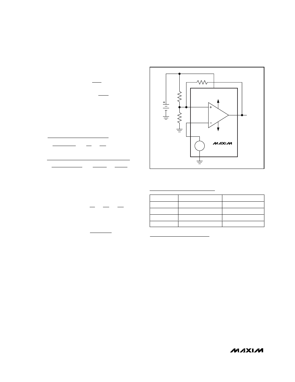
V
REF
R3
R1
R2
V
BATT
V
BGOOD
V
SS
V
SS
V
DD
V
DD
IN+
REF
IN-
OUT
MAX4037
Figure 4. Battery Monitoring
Selector Guide
PART
NO. OF AMPLIFIERS
REFERENCE
MAX4036
1
—
MAX4037
1
√
MAX4038
2
—
MAX4039
2
√