Bias, Applications information – Rainbow Electronics MAX4039 User Manual
Page 11
MAX4036–MAX4039
Low I
BIAS
, +1.4V/800nA, Rail-to-Rail Op Amps
with +1.2V Buffered Reference
______________________________________________________________________________________
11
Applications Information
Power-Supply Considerations
The MAX4036–MAX4039 operate from a single 1.4V
(MAX4036/MAX4038) or 1.8V (MAX4037/MAX4039) to
3.6V supply. A high amplifier power-supply rejection
ratio of 82dB and the excellent reference line regulation
allow the devices to be powered directly from a decay-
ing battery voltage, simplifying design and extending
battery life. The MAX4036–MAX4039 are ideally suited
for low-voltage battery-powered systems. The Typical
Operating Characteristics show the changes in supply
current and reference output as a function of supply
voltage.
Power-Up Settling Time
The MAX4036–MAX4039 typically require 0.25ms to
power-up. During this startup time, the output is inde-
terminate. The application circuit should allow for this
initial delay. See the Typical Operating Characteristics
for amplifier and reference settling time curves.
Driving Capacitive Loads: Op Amps
The MAX4036–MAX4039 amplifier(s) require no output
capacitor for stability, and are unity-gain stable for
loads up to 5000pF. Applications that require greater
capacitive-drive capability should use an isolation
resistor between the output and the capacitive load
(Figure 2). Note that this solution reduces the gain and
output voltage swing because R
ISO
forms a voltage-
divider with the load resistor.
Crossover Distortion
The MAX4036–MAX4039 output stages are capable of
sourcing and sinking currents with orders of magnitude
greater than the stages’ quiescent current, which is
less than 1µA. This ability to drive heavy loads with
such a small quiescent current introduces crossover
distortion as the output stage passes between sinking
and sourcing. In the crossover regions, the output
impedance of the MAX4036–MAX4039 increases sub-
stantially, thereby changing the load-driving character-
istics. The distortion can be greatly reduced by
increasing the load resistance. For applications where
low load resistance is required, bias the load such that
the output current is always in one direction, to avoid
crossover distortion.
Reference Bypassing
The MAX4037/MAX4039 reference requires no external
capacitors.
Using the MAX4036–MAX4039 as a
Comparator
Although optimized for use as an operational amplifier,
the MAX4036–MAX4039 can be used as a rail-to-rail
I/O comparator (Figures 3, 4). External hysteresis can
be used to minimize the risk of output oscillation. The
positive feedback circuit, shown in Figure 4, causes the
input threshold to change when the output voltage
changes state.
Battery Monitoring Using the
MAX4037/MAX4039 and Hysteresis
The internal reference and low operating voltage of the
MAX4037/MAX4039 make the devices ideal for battery-
monitoring applications. Hysteresis can be set using
resistors as shown in Figure 4, and the following design
procedure:
1)
Choose R3. The input bias current of IN_+ is under
100pA over temperature, so a current through R3
around 100nA maintains accuracy. The current
through R3 at the trip point is V
REF
/ R3, or 100nA
for R3 = 12MΩ. 10MΩ is a good practical value.
2)
Choose the hysteresis voltage (V
HB
), the voltage
between the upper and lower thresholds. In this
example, choose V
HB
= 50mV (see Figure 3).
MAX4038
R
ISO
R
L
C
L
R
L
R
L
+ R
ISO
A
V
=
= 1
Figure 2. Using a Resistor to Isolate a Capacitive Load from
the Op Amp
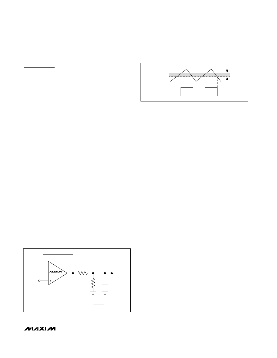
V
HB
V
OH
V
OL
V
THR
V
THF
INPUT
OUTPUT
Figure 3. Hysteresis