Supply bypassing and board layout, Capacitive-load stability – Rainbow Electronics MAX4284 User Manual
Page 14
MAX4174/5, MAX4274/5, MAX4281/2/4
SOT23, Rail-to-Rail, Fixed-Gain
GainAmps/Open-Loop Op Amps
14
______________________________________________________________________________________
MAX4174
V
EE
V
CC
R
G
R
F
R
ISO
C
L
R
L
OUTPUT
INPUT
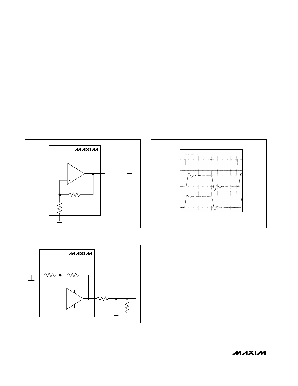
Figure 9. Dual-Supply, Capacitive-Load Driving Circuit
Figure 10. Small-Signal/Large-Signal Transient Response with
Excessive Capacitive Load with Isolation Resistor
A
V
= +5V/V
50mV/div
INPUT
OUTPUT
OUTPUT
A
V
= +5V/V
500mV/div
Supply Bypassing and Board Layout
All devices in the GainAmp family operate from a +2.5V
to +5.5V single supply or from ±1.25V to ±2.75V dual
supplies. For single-supply operation, bypass the
power supply with a 0.1µF capacitor to ground. For
dual supplies, bypass each supply to ground. Bypass
with capacitors as close to the device as possible, to min-
imize lead inductance and noise. A printed circuit board
with a low-inductance ground plane is recommended.
Capacitive-Load Stability
Driving large capacitive loads can cause instability in
most low-power, rail-to-rail output amplifiers. The fixed-
gain amplifiers of this GainAmp family are stable with
capacitive loads up to 470pF. Stability with higher
capacitive loads can be improved by adding an isolation
resistor in series with the op-amp output, as shown in
Figure 9. This resistor improves the circuit’s phase mar-
gin by isolating the load capacitor from the amplifier’s
output. In Figure 10, a 1000pF capacitor is driven with a
100
Ω
isolation resistor exhibiting some overshoot but no
oscillation. Figures 11 and 12 show the typical small-sig-
nal pulse responses of GainAmp fixed-gain amplifiers
with 250pF and 470pF capacitive loads and no isolation
resistor.
MAX4174
V
EE
V
CC
R
G
R
F
V
IN
V
OUT
= V
IN
(
1+
R
F
)
R
G
Figure 8. Dual-Supply, DC-Coupled Noninverting Amplifier