Typical operating characteristics (continued), Pin descriptions – Rainbow Electronics MAX5071 User Manual
Page 9
MAX5070/MAX5071
High-Performance, Single-Ended, Current-Mode
PWM Controllers
_______________________________________________________________________________________
9
OUT SOURCE AND SINK CURRENTS
MAX5070 toc20
V
CC
= 15V
I
OUT
2A/div
V
OUT
10V/div
20Ons/div
C
OUT
= 10nF
2
4
3
5
8
9
7
6
10
20
220 320 420 520
120
620 720 820 920 1020
SUPPLY CURRENT (I
CC
)
vs. OSCILLATOR FREQUENCY (C
T
= 100pF)
MAX5070 toc21
FREQUENCY (kHz)
SUPPLY CURRENT (mA)
T
A
= +125°C
T
A
= +85°C
T
A
= +25°C
T
A
= -40°C
MAX5070A/MAX5071A
MAXIMUM DUTY CYCLE vs. R
T
MAX5070 toc22
R
T
(Ω)
DUTY CYCLE (%)
10k
1k
30
40
50
60
70
80
90
100
20
100
100k
C
T
= 1nF
C
T
= 560pF
C
T
= 220pF
C
T
= 100pF
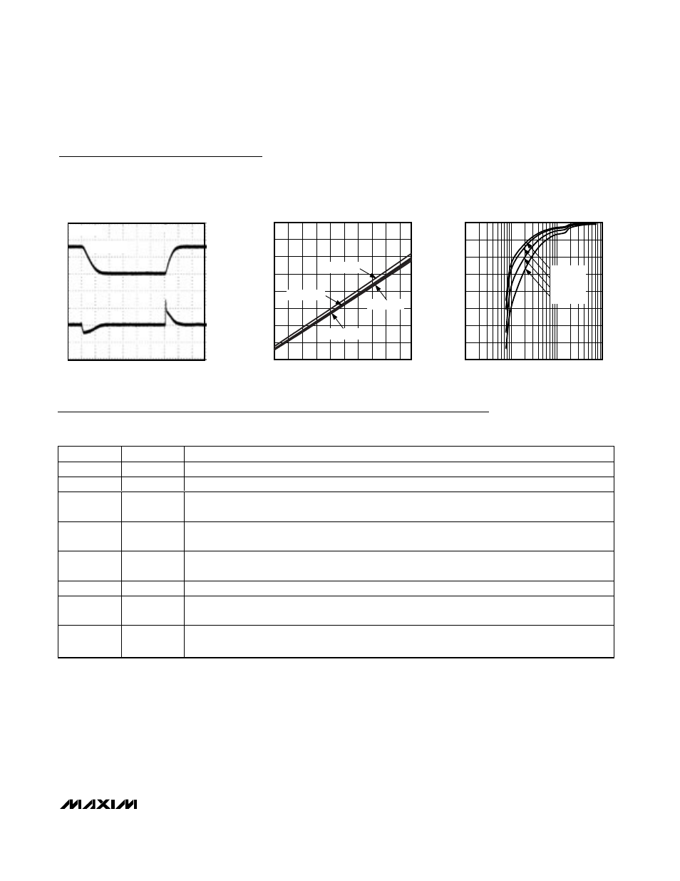
Typical Operating Characteristics (continued)
(V
CC
= 15V, T
A
= +25°C, unless otherwise noted.)
Pin Descriptions
PIN
NAME
FUNCTION
1
COMP
Error-Amplifier Output. COMP can be used for soft-start.
2
FB
Error-Amplifier Inverting Input
3
CS
Input to the PWM Comparator and Overcurrent Protection Comparator. The current-sense signal is
compared to a signal proportional to the error-amplifier output voltage.
4
R
T
/C
T
Timing Resistor and Capacitor Connection. A resistor R
T
from R
T
/C
T
to VREF and capacitor C
T
from
R
T
/C
T
to GND set the oscillator frequency.
5
GND
Power-Supply Ground. Place the V
CC
and VREF bypass capacitors close to the IC to minimize
ground loops.
6
OUT
MOSFET Driver Output. OUT connects to the gate of the external n-channel MOSFET.
7
V
CC
Power-Supply Input for MAX5070. Bypass V
CC
to GND with a 0.1µF ceramic capacitor or a parallel
combination of a 0.1µF and a higher value ceramic capacitor.
8
VREF
5V Reference Output. Bypass VREF to GND with a 0.1µF ceramic capacitor or a parallel combination
of a 0.1µF and a higher value ceramic capacitor.
MAX5070A/MAX5070B