Pin descriptions (continued) – Rainbow Electronics MAX5071 User Manual
Page 10
MAX5070/MAX5071
High-Performance, Single-Ended, Current-Mode
PWM Controllers
10
______________________________________________________________________________________
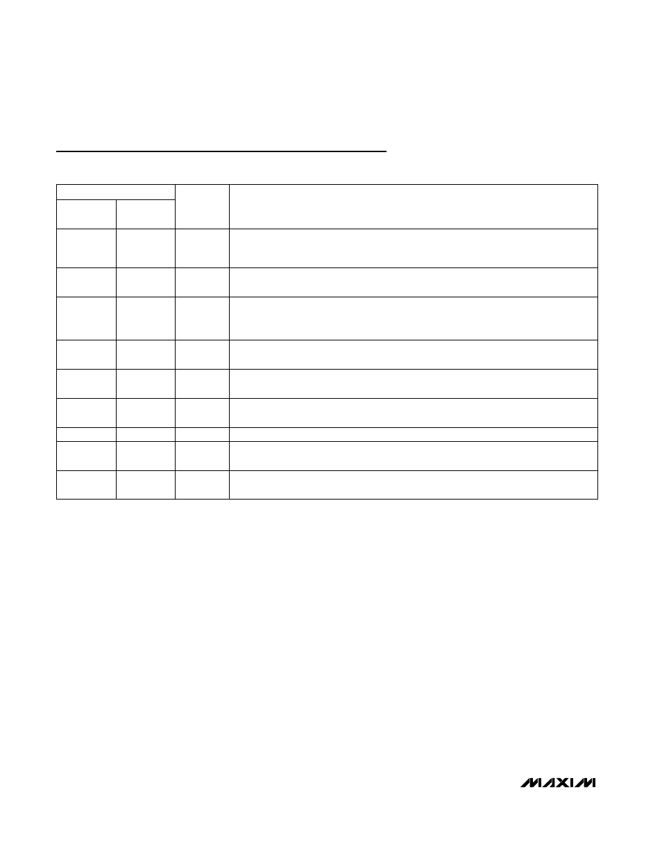
Pin Descriptions (continued)
PIN
MAX5071A/
MAX5071B
MAX5071C
NAME
FUNCTION
1
1
COMP
COMP is level-shifted and connected to the inverting input of the PWM comparator. Pull
up COMP to VREF through a resistor and connect an optocoupler from COMP to GND for
proper operation.
2
—
SYNC
Bidirectional Synchronization Input. When synchronizing with other
MAX5071A/MAX5071Bs, the higher frequency part synchronizes all other devices.
—
2
ADV_CLK
ADV_CLK is an 85ns clock output pulse preceding the rising edge of OUT (see Figure 4).
Use the pulse to drive the secondary-side synchronous rectifiers through a pulse
transformer or an optocoupler (see Figure 8).
3
3
CS
Input to the PWM Comparator and Overcurrent Protection Comparator. The current-
sense signal is compared to the voltage at COMP.
4
4
R
T
/C
T
Timing Resistor and Capacitor Connection. A resistor R
T
from R
T
/C
T
to VREF and
capacitor C
T
from R
T
/C
T
to GND set the oscillator frequency.
5
5
GND
Power-Supply Ground. Place the V
CC
and VREF bypass capacitors close to the IC to
minimize ground loops.
6
6
OUT
MOSFET Driver Output. OUT connects to the gate of the external n-channel MOSFET.
7
7
V
CC
Power-Supply Input for MAX5071. Bypass V
CC
to GND with a 0.1µF ceramic capacitor or
a parallel combination of a 0.1µF and a higher value ceramic capacitor.
8
8
V
REF
5V Reference Output. Bypass VREF to GND with a 0.1µF ceramic capacitor or a parallel
combination of a 0.1µF and a higher value ceramic capacitor.
MAX5071A/MAX5071B/MAX5071C