Rainbow Electronics MAX5071 User Manual
Page 2
MAX5070/MAX5071
High-Performance, Single-Ended, Current-Mode
PWM Controllers
2
_______________________________________________________________________________________
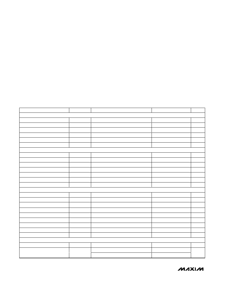
ABSOLUTE MAXIMUM RATINGS
ELECTRICAL CHARACTERISTICS
(V
CC
= +15V, R
T
= 10kΩ, C
T
= 3.3nF, V
VREF
= OPEN, C
VREF
= 0.1µF, COMP = OPEN, V
FB
= 2V, CS = GND,
T
A
= -40°C to +85°C
,
unless otherwise noted.) (Note 1)
Stresses beyond those listed under “Absolute Maximum Ratings” may cause permanent damage to the device. These are stress ratings only, and functional
operation of the device at these or any other conditions beyond those indicated in the operational sections of the specifications is not implied. Exposure to
absolute maximum rating conditions for extended periods may affect device reliability.
V
CC
(Low-Impedance Source) to GND ..................-0.3V to +30V
V
CC
(I
CC
< 30mA).....................................................Self Limiting
OUT to GND ...............................................-0.3V to (V
CC
+ 0.3V)
OUT Current.............................................................±1A for 10µs
FB, SYNC, COMP, CS, R
T
/C
T
, VREF to GND ...........-0.3V to +6V
COMP Sink Current (MAX5070)..........................................10mA
Continuous Power Dissipation (T
A
= +70°C)
8-Pin µMAX (derate 4.5mW/°C above +70°C) .............362mW
8-Pin SO (derate 5.9mW/°C above +70°C)...............470.6mW
Operating Temperature Range (Automotive) ....-40°C to +125°C
Maximum Junction Temperature .....................................+150°C
Storage Temperature Range .............................-65°C to +150°C
Lead Temperature (soldering, 10s) .................................+300°C
PARAMETER
SYMBOL
CONDITIONS
MIN
TYP
MAX
UNITS
REFERENCE
Output Voltage
V
VREF
T
A
= +25°C, I
VREF
= 1mA
4.950
5.000
5.050
V
Line Regulation
∆
V
LINE
12V < V
CC
< 25V, I
VREF
= 1mA
0.4
4
mV
Load Regulation
∆
V
LOAD
1mA < I
VREF
< 20mA
6
25
mV
Total Output Variation
V
REFT
1mA < I
VREF
< 20mA, 12V < V
CC
< 25V
4.9
5.1
V
Reference Output-Noise Voltage
V
NOISE
10Hz < f < 10kHz, T
A
= +25°C
50
µV
Reference Output Short Circuit
I
S_SC
V
VREF
=
0V
-30
-100
-180
mA
OSCILLATOR
Initial Accuracy
T
A
= +25°C
51
54
57
kHz
Voltage Stability
12V < V
CC
< 25V
0.2
0.5
%
Temp Stability
-40°C < T
A
< +85°C
0.5
%
R
T
/C
T
Voltage Ramp (
P-P
)
V
RAMP
1.7
V
R
T
/C
T
Voltage Ramp Valley
V
RAMP_VALLEY
1.1
V
Discharge Current
I
DIS
V
RT/CT
= 2V, T
A
= +25°C
7.9
8.3
8.7
mA
Frequency Range
f
OSC
20
1000
kHz
ERROR AMPLIFIER (MAX5070A/MAX5070B)
FB Input Voltage
V
FB
FB shorted to COMP
2.465
2.5
2.535
V
FB Input Bias Current
I
B(FB)
-0.01
-0.1
µA
Open-Loop Voltage Gain
A
VOL
2V
≤
V
COMP
≤
4V
100
dB
Unity-Gain Bandwidth
f
GBW
1
MHz
Power-Supply Rejection Ratio
PSRR
12V
≤
V
CC
≤
25V (Note 2)
60
80
dB
COMP Sink Current
I
SINK
V
FB
= 2.7V, V
COMP
= 1.1V
2
6
mA
COMP Source Current
I
SOURCE
V
FB
= 2.3V, V
COMP
= 5V
-0.5
-1.2
-1.8
mA
COMP Output High Voltage
V
COMPH
V
FB
= 2.3V, R
COMP
= 15k
Ω
to GND
5
5.8
V
COMP Output Low Voltage
V
COMPL
V
FB
= 2.7V, R
COMP
= 15k
Ω
to VREF
0.1
1.1
V
CURRENT-SENSE AMPLIFIER
Gain
A
CS
(Notes 3, 4)
2.85
3
3.26
V/V
MAX5070A/B (Note 3)
0.95
1
1.05
Maximum Current-Sense Signal
V
CS_MAX
V
COMP
= 5V, MAX5071_
0.84
0.935
1.03
V