Ac electrical characteristics – Rainbow Electronics ADC1251 User Manual
Page 5
AC Electrical Characteristics
(Continued)
The following specifications apply for DV
CC
e
AV
CC
e
a
5 0V V
b
e
b
5 0V t
r
e
t
f
e
20 ns unless otherwise specified
Boldface limits apply for T
A
e
T
J
e
T
MIN
to T
MAX
all other limits T
A
e
T
J
e
25 C (Notes 6 and 7)
Symbol
Parameter
Conditions
Typical
Limit
Units
(Note 9)
(Note 10 19)
(Limit)
t
A
Acquisition Time
R
SOURCE
e
50X
3 5
3 5
m
s(min)
(Note 15)
t
IA
Internal Acquisition Time
7(1 f
CLK
)
7(1 f
CLK)
(max)
(when using WR Control Only)
t
ZA
Auto Zero Time a
33(1 f
CLK
)
33(1 f
CLK
) a 250 ns
(max)
Acquisition Time
f
CLK
e
1 75 MHz
18 8
19 05
m
s(max)
t
D(EOC)L
Delay from Hold Command
Using WR Control
200
350
ns(max)
to Falling Edge of EOC
Using S H Control
100
150
ns(max)
t
CAL
Calibration Time
1399 (1 f
CLK
)
1399 (1 f
CLK
)
(max)
f
CLK
e
3 5 MHz
399
400
m
s(max)
t
W(CAL)L
Calibration Pulse Width
(Note 16)
60
200
ns(min)
t
W(WR)L
minimum WR Pulse Width
60
200
ns(min)
t
ACC
maximum Access Time
C
L
e
100 pF
(Delay from Falling Edge of
50
95
ns(max)
RD to Output Data Valid)
t
0H
t
1H
TRI-STATE Control (Delay
R
L
e
1 kX
from Rising Edge of RD
C
L
e
100 pF
30
70
ns(max)
to Hi-Z State)
t
PD(INT)
maximum Delay from Falling Edge
100
175
ns(max)
of RD or WR to Reset of INT
t
RR
Delay between Successive RD Pulses
30
60
ns(min)
Note 1
Absolute Maximum Ratings indicate limits beyond which damage to the device may occur Operating Ratings indicate conditions for which the device is
functional but do not guarantee specific performance limits For guaranteed specifications and test conditions see the Electrical Characteristics The guaranteed
specifications apply only for the test conditions listed Some performance characteristics may degrade when the device is not operated under the listed test
conditions
Note 2
All voltages are measured with respect to AGND and DGND unless otherwise specified
Note 3
When the input voltage (V
IN
) at any pin exceeds the power supply rails (V
IN
k
V
b
or V
IN
l
(AV
CC
or DV
CC
) the current at that pin should be limited to
5 mA The 20 mA maximum package input current rating allows the voltage at any four pins with an input current limit of 5 mA to simultaneously exceed the power
supply voltages
Note 4
The power dissipation of this device under normal operation should never exceed 191 mW (Quiescent Power Dissipation
a
1 TTL Load on each digital
output) Caution should be taken not to exceed absolute maximum power rating when the device is operating in a severe fault condition (ex when any inputs or
outputs exceed the power supply) The maximum power dissipation must be derated at elevated temperatures and is dictated by T
JMax
(maximum junction
temperature) i
JA
(package junction to ambient thermal resistance) and T
A
(ambient temperature) The maximum allowable power dissipation at any temperature
is P
DMax
e
(T
JMax
b
T
A
) i
JA
or the number given in the Absolute Maximum Ratings whichever is lower For this device T
JMax
e
150 C and the typical thermal
resistance (i
JA
) of the ADC12451 with CMJ and CIJ suffixes when board mounted is 51 C W
Note 5
Human body model 100 pF discharged through a 1 5 kX resistor
Note 6
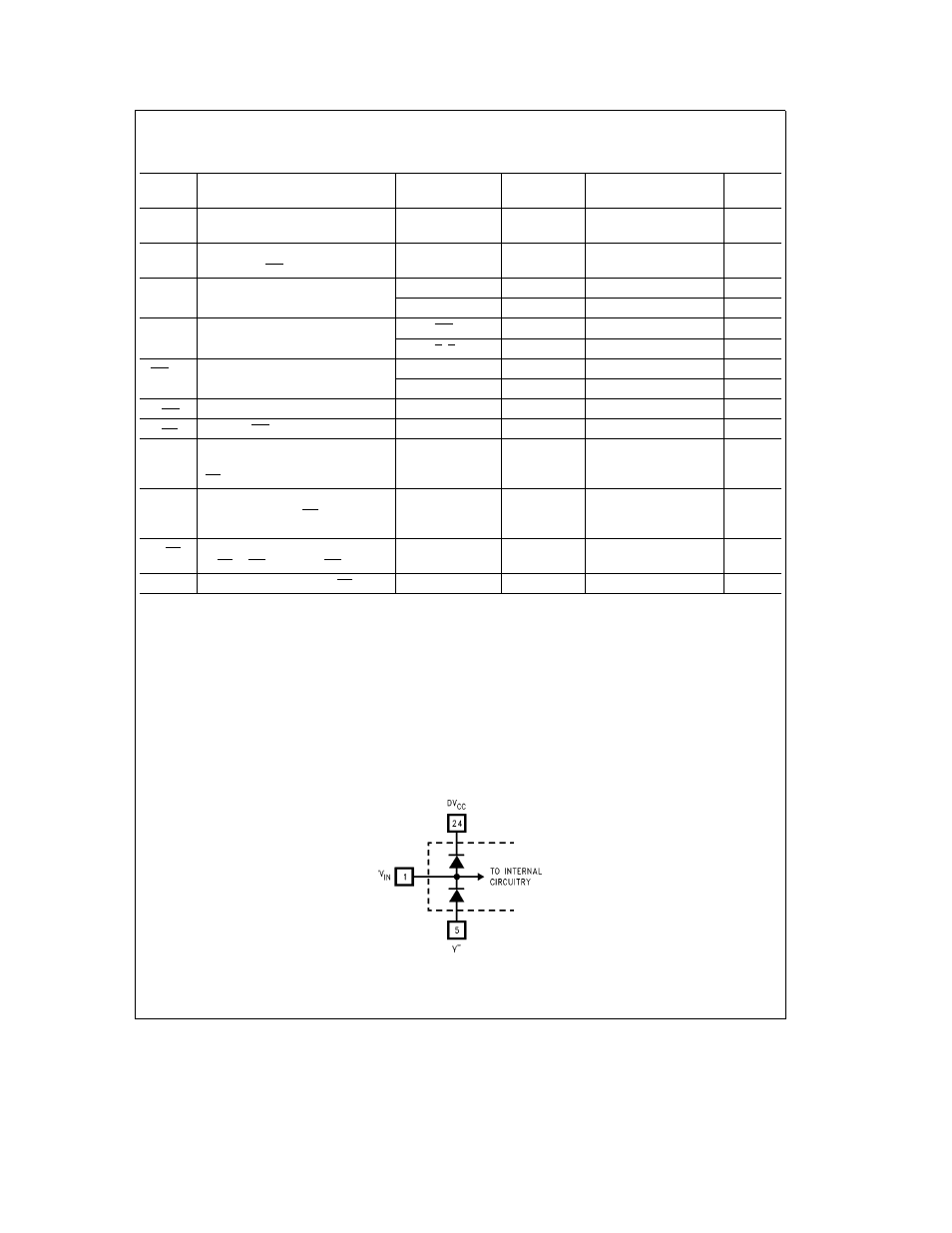
Two on-chip diodes are tied to the analog input as shown below Errors in the A D conversion can occur if these diodes are forward biased more than
50 mV This means that if AV
CC
and DV
CC
are minimum (4 75 V
DC
) and V
b
is maximum (
b
4 75 V
DC
) the analog input full-scale voltage must be
s g
4 8 V
DC
TL H 11025 – 4
5