3 0 analog considerations – Rainbow Electronics ADC1251 User Manual
Page 14
3 0 Analog Considerations
(Continued)
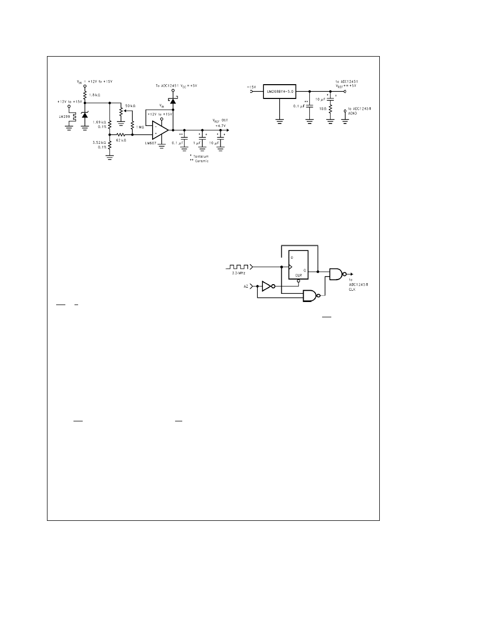
TL H 11025 – 20
FIGURE 4a Low Drift Extremely Stable Reference Circuit
TL H 11025 – 21
Errors without any trims
25 C
b
40 C to a85 C
Full Scale
g
0 075%
g
0 2%
Zero
g
0 024%
g
0 024%
Linearity
g
LSB
g
LSB
FIGURE 4b Simple Reference Circuit
In a ratiometric system the analog input voltage is propor-
tional to the voltage used for the A D reference When this
voltage is the system power supply the V
REF
pin can be
tied to V
CC
This technique relaxes the stability requirement
of the system reference as the analog input and A D refer-
ence move together maintaining the same output code for a
given input condition
For absolute accuracy where the analog input varies be-
tween very specific voltage limits the reference pin can be
biased with a time and temperature stable voltage source
In general the magnitude of the reference voltage will re-
quire an initial adjustment to null out full-scale errors
3 2 ACQUISITION WINDOW
As shown in the timing diagrams there are three different
methods of starting a conversion each of which affects the
acquisition window and timing
With Auto-Zero high a conversion can be started with the
WR or S H controls In either method of starting a conver-
sion the rising edge of EOC signals the actual beginning of
the acquisition window At this time a voltage spike may be
noticed on the analog input of the ADC12451 whose ampli-
tude is dependent on the input voltage and the source re-
sistance The timing diagrams for these two methods of
starting a conversion do not show the acquisition window
starting at this time because the acquisition time (t
A
) must
start after the conversion result high and low bytes have
been read This is necessary since activating and deactivat-
ing the digital outputs (DB0 DB7 – DB8 DB12) causes cur-
rent fluctuations in the ADC12451’s internal DV
CC
lines
This generates digital noise which couples into the capaci-
tive ladder that stores the analog input voltage Therefore
the time interval between the rising edge of EOC and the
second read is inappropriate for analog input voltage acqui-
sition
When WR is used to start a conversion with AZ low the
Auto-Zero cycle is inserted before the acquisition window In
this method the acquisition window is internally controlled
by the ADC12451 and lasts for approximately 7 clock peri-
ods Since the acquisition window needs to be at least
3 5 ms at all times when using Auto-Zero the maximum
clock frequency is limited to 2 MHz The zero error with the
Auto-Zero cycle is production tested at a clock frequency of
1 75 MHz This accommodates easy switching between a
conversion with the Auto-Zero cycle (f
CLK
e
1 75 MHz) and
without (f
CLK
e
3 5 MHz) as shown in
Figure 5
TL H 11025 – 22
FIGURE 5 Switching between a Conversion with and
without Auto-Zero when Using WR Control
3 3 INPUT CURRENT
Because the input network of the ADC12451 is made up of
a switch and a network of capacitors a charging current will
flow into or out of (depending on the input voltage polarity)
of the analog input pin (V
IN
) on the start of the analog input
sampling period The peak value of this current will depend
on the actual input voltage applied and the source resist-
ance
3 4 NOISE
The leads to the analog input pin should be kept as short as
possible to minimize input noise coupling Both noise and
undesired digital clock coupling to this input can cause er-
rors Input filtering can be used to reduce the effects of
these noise sources
14