Absolute maximum ratings, Operating ratings, Converter electrical characteristics – Rainbow Electronics ADC1251 User Manual
Page 2
Absolute Maximum Ratings
(Notes 1
2)
If Military Aerospace specified devices are required
please contact the National Semiconductor Sales
Office Distributors for availability and specifications
Supply Voltage (V
CC
e
DV
CC
e
AV
CC
)
6 5V
Negative Supply Voltage (V
b
)
b
6 5V
Voltage at Logic Control Inputs
b
0 3V to (V
CC
a
0 3V)
Voltage at Analog Inputs
(V
IN
V
REF
)
(V
b
b
0 3V) to (V
CC
a
0 3V)
AV
CC
-DV
CC
(Note 7)
0 3V
Input Current at any Pin (Note 3)
g
5 mA
Package Input Current (Note 3)
g
20 mA
Power Dissipation at 25 C (Note 4)
875 mW
Storage Temperature Range
b
65 C to a150 C
ESD Susceptability (Note 5)
2000V
Soldering Information
J Package (10 Seconds)
300 C
Operating Ratings
(Notes 1
2)
Temperature Range
T
MIN
s
T
A
s
T
MAX
ADC12451CIJ
b
40 C
s
T
A
s
a
85 C
ADC12451CMJ
ADC12451CMJ 883
b
55 C
s
T
A
s
a
125 C
DV
CC
and AV
CC
Voltage
(Notes 6
7)
4 5V to 5 5V
Negative Supply Voltage (V
b
)
b
4 5V to b5 5V
Reference Voltage
(V
REF
Notes 6
7)
3 5V to AV
CC
a
50 mV
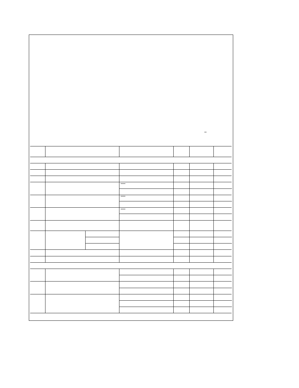
Converter Electrical Characteristics
The following specifications apply for V
CC
e
DV
CC
e
AV
CC
e a
5 0V V
b
e b
5 0V V
REF
e a
5 0V using S H input for
conversion control and f
CLK
e
3 5 MHz unless otherwise specified Boldface limits apply for T
A
e
T
J
e
T
MIN
to T
MAX
all
other limits T
A
e
T
J
e
25 C (Notes 6 7 and 8)
Symbol
Parameter
Conditions
Typical
Limit
Units
(Note 9)
(Note 10 19)
(Limit)
STATIC CHARACTERISTICS
Positive Integral Linearity Error
After Auto-Cal (Notes 11
12)
g
LSB
Negative Integral Linearity Error
After Auto-Cal (Notes 11
12)
g
LSB
Positive or Negative Differential Linearity
After Auto-Cal (Notes 11
12)
12
Bits
Zero Error (Notes 12
13)
AZ e ‘‘0’’ f
CLK
e
1 75 MHz
g
1
LSB
After Auto-Cal Only
g
2
g
3 0
LSB(max)
Positive Full-Scale Error (Note 12)
AZ e ‘‘0’’ f
CLK
e
1 75 MHz
g
1
LSB
Auto-Cal Only
g
1 5
g
2 5
LSB(max)
Negative Full-Scale Error (Note 12)
AZ e ‘‘0’’ f
CLK
e
1 75 MHz
g
1
LSB
Auto-Cal Only
g
1 5
g
3 0
LSB(max)
V
IN
Analog Input Voltage
V
b
b
0 05
V(min)
V
CC
a
0 05
V(max)
Power Supply Sensitivity
Zero Error (Note 14) AV
CC
e
DV
CC
e
5V
g
5%
g
LSB
Full-Scale Error
V
REF
e
4 75V V
b
e b
5V
g
5%
g
LSB
Linearity Error
g
LSB
C
REF
V
REF
Input Capacitance
80
pF
C
IN
Analog Input Capacitance
65
pF
DYNAMIC CHARACTERISTICS
Bipolar Effective Bits (Note 17)
f
IN
e
1 kHz V
IN
e
g
4 85V
12 6
Bits
f
IN
e
20 67 kHz V
IN
e
g
4 85V
12 6
11 9
Bits(min)
Unipolar Effective Bits (Note 17)
f
IN
e
1 kHz V
IN
e
4 85 V
p-p
11 8
Bits
f
IN
e
20 67 kHz V
IN
e
4 85 V
p-p
11 8
11 1
Bits(min)
S N
Bipolar Signal to Noise Ratio (Note 17)
f
IN
e
1 kHz V
IN
e
g
4 85V
78
dB
f
IN
e
10 kHz V
IN
e
g
4 85V
78
dB
f
IN
e
20 67 kHz V
IN
e
g
4 85V
78
73 5
dB(min)
2