2 0 functional description, 3 0 analog considerations – Rainbow Electronics ADC1251 User Manual
Page 13
2 0 Functional Description
(Continued)
A conversion sequence can also be controlled by the S H
and CS inputs Taking CS and S H low starts the acquisition
window for the analog input voltage The rising edge of S H
immediately puts the A D in the hold mode and starts the
conversion Using S H will simplify synchronizing the end of
the acquisition window to other signals which may be nec-
essary in a DSP environment
During a conversion the sampled input voltage is succes-
sively compared to the output of the DAC First the ac-
quired input voltage is compared to analog ground to deter-
mine its polarity The sign bit is set low for positive input
voltages and high for negative Next the MSB of the DAC is
set high with the rest of the bits low If the input voltage is
greater than the output of the DAC then the MSB is left
high otherwise it is set low The next bit is set high making
the output of the DAC three quarters or one quarter of full
scale A comparison is done and if the input is greater than
the new DAC value this bit remains high if the input is less
than the new DAC value the bit is set low This process
continues until each bit has been tested The result is then
stored in the output latch of the ADC12451 Next INT goes
low and EOC goes high to signal the end of the conversion
The result can now be read by taking CS and RD low to
enable the DB0 DB8 – DB7 DB12 output buffers The high
byte of data is relayed first on the data bus outputs as
shown below
DB0
DB1
DB2
DB3
DB4
DB5
DB6
DB7
DB8
DB9
DB10
DB11
DB12
DB12
DB12
DB12
Bit 8
Bit 9
Bit 10
MSB
Sign Bit
Sign Bit
Sign Bit
Sign Bit
Taking CS and RD low a second time will relay the low byte
of data on the data bus outputs as shown below
DB0
DB1
DB2
DB3
DB4
DB5
DB6
DB7
DB8
DB9
DB10
DB11
DB12
DB12
DB12
DB12
LSB
Bit 1
Bit 2
Bit 3
Bit 4
Bit 5
Bit 6
Bit 7
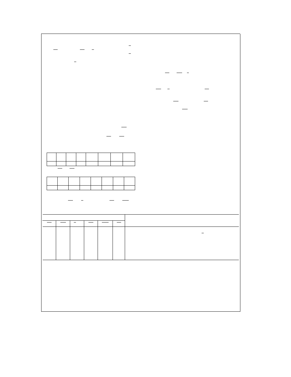
The table in
Figure 3
summarizes the effect of the digital
control inputs on the function of the ADC12451 The Test
Mode where RD and S H are high and CS and CAL are
low is used during manufacture to thoroughly check out
the operation of the ADC12451 Care should be taken not to
inadvertently be in this mode since DB2 DB3 DB5 and
DB6 become active outputs which may cause data bus
contention
2 2 RESETTING THE A D
The ADC12451 is reset whenever a new conversion is start-
ed by taking CS and WR or S H low If this is done when the
analog input is being sampled or when EOC is low the
Auto-Cal correction factors may be corrupted therefore re-
quiring an Auto-Cal cycle before the next conversion When
using WR or S H without Auto-Zero (AZ e 1) to start a
conversion a new conversion can be restarted only after
EOC has gone high signaling the end of the current conver-
sion When using WR with Auto-Zero (AZ e 0) a new con-
version can be restarted during the first 26 clock periods
after the rising edge of WR (t
Z
) or after EOC has returned
high without corrupting the Auto-Cal correction factors
The Calibration Cycle cannot be reset once started On
power-up the ADC12451 automatically goes through a Cali-
bration Cycle that takes typically 1399 clock cycles For rea-
sons that will be discussed in Section 3 8 a new calibration
cycle needs to be started after the completion of the auto-
matic one
3 0 Analog Considerations
3 1 REFERENCE VOLTAGE
The voltage applied to the reference input of the converter
defines the voltage span of the analog input (the difference
between V
IN
and AGND) over which 4095 positive output
codes and 4096 negative output codes exist The A-to-D
can be used in either ratiometric or absolute reference ap-
plications The voltage source driving V
REF
must have a
very low output impedance and very low noise The circuit in
Figure 4a
is an example of a very stable reference that is
appropriate for use with the ADC12451 The simple refer-
ence circuit of
Figure 4b
may be used when the application
does not require a low full-scale error
Digital Control Inputs
A D Function
CS
WR
S H
RD
CAL
AZ
1
1
1
1
Start Conversion without Auto-Zero
1
1
1
1
Start Conversion synchronous with rising edge of S H without Auto-Zero
1
1
1
1
Read Conversion Result without Auto-Zero
1
1
1
0
Start Conversion with Auto-Zero
1
1
1
0
Read Conversion Result with Auto-Zero
1
X
1
X
X
Start Calibration Cycle
0
X
X
1
0
X
Test Mode (DB2 DB3 DB5 and DB6 become active)
FIGURE 3 Function of the A D Control Inputs
13