High-voltage switch control – Rainbow Electronics MAX17075 User Manual
Page 16
MAX17075
Boost Regulator with Integrated Charge Pumps,
Switch Control, and High-Current Op Amp
16
______________________________________________________________________________________
Short-Circuit Current Limit and Input Clamp
The operational amplifier limits short-circuit current to
approximately ±500mA if the output is directly shorted
to SUP or to BGND. If the short-circuit condition per-
sists, the junction temperature of the IC rises until it
reaches the thermal-shutdown threshold (+160°C typ).
Once the junction temperature reaches the thermal-
shutdown threshold, an internal thermal sensor immedi-
ately sets the thermal fault latch, shutting off all the IC’s
outputs. The device remains inactive until the input volt-
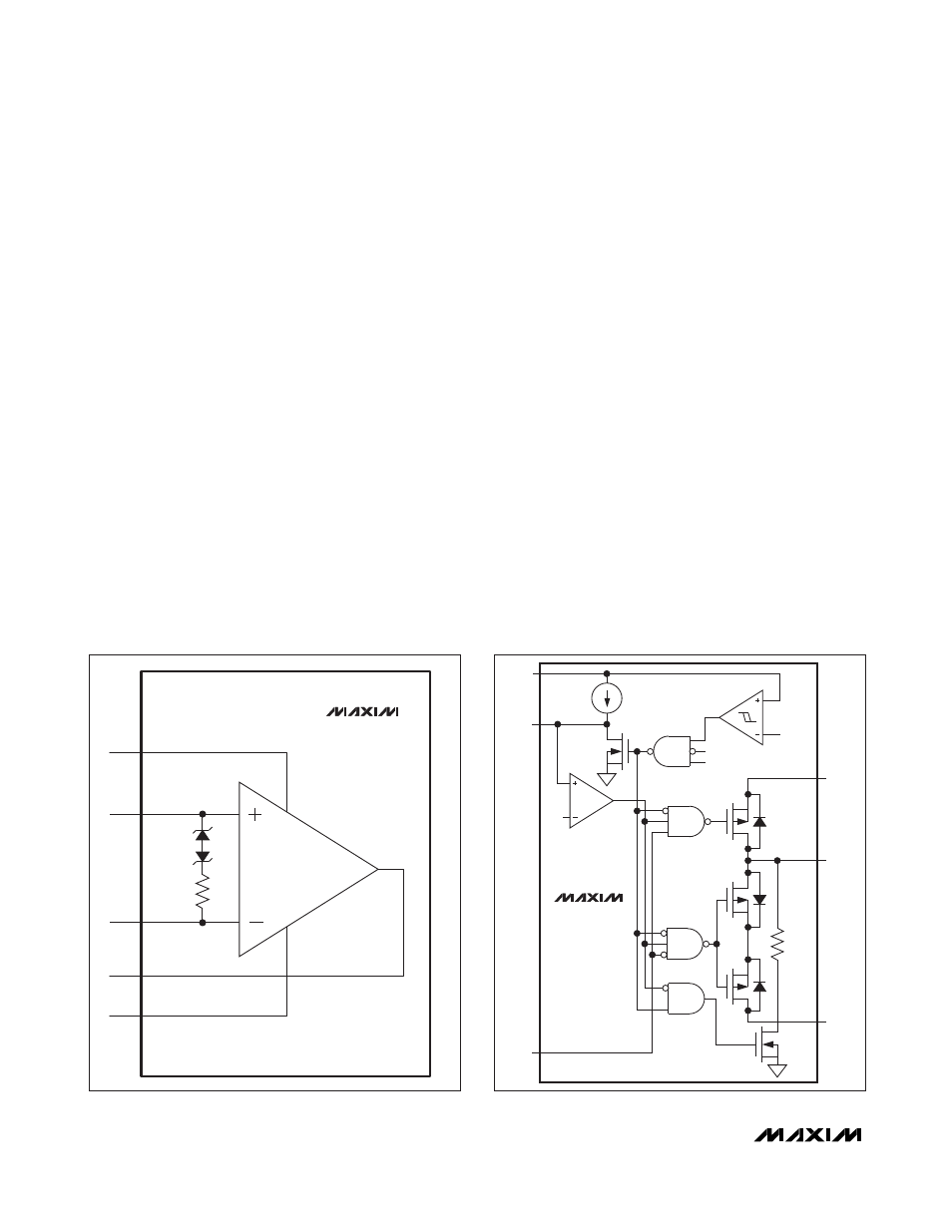
age is cycled. The operational amplifier has 4V input
clamp structures in series with a 500
Ω resistance and a
diode (Figure 6).
Driving Pure Capacitive Load
The operational amplifier is typically used to drive the
LCD backplane (VCOM) or the gamma-correction
divider string. The LCD backplane consists of a distrib-
uted series capacitance and resistance, a load that can
be easily driven by the operational amplifier. However,
if the operational amplifier is used in an application with
a pure capacitive load, steps must be taken to ensure
stable operation. As the operational amplifier’s capaci-
tive load increases, the amplifier’s bandwidth decreas-
es and gain peaking increases. A 5
Ω to 50Ω small
resistor placed between OUT and the capacitive load
reduces peaking, but also reduces the gain. An alterna-
tive method of reducing peaking is to place a series RC
network (snubber) in parallel with the capacitive load.
The RC network does not continuously load the output
or reduce the gain. Typical values of the resistor are
between 100
Ω and 200Ω, and the typical value of the
capacitor is 10nF.
High-Voltage Switch Control
The MAX17075’s high-voltage switch control block
(Figure 7) consists of two high-voltage p-channel
MOSFETs: Q1, between SRC and COM; and Q2,
between COM and DRN. At power-up and only at
power up, before the switch control is enabled (a 1.5k
Ω
pulldown is present on COM). At switch-off, COM is
high impedance.
The switch control input (CTL) is not activated until all
four of the following conditions are satisfied: the input
voltage exceeds UVLO, the soft-start routine of all the
regulators is complete, there is no fault condition
detected, and V
DEL
exceeds its turn-on threshold.
Once activated and if CTL is logic-high, Q1 turns on
and Q2 turns off, connecting COM to SRC. When CTL
is logic-low, Q1 turns off and Q2 turns on, connecting
COM to DRN.
Figure 6. Op Amp Input Clamp Structure
NEG
POS
±4V
500
Ω
OP AMP INPUT CLAMP STRUCTURE
SUP
OUT
BGND
MAX17075
Figure 7. Switch Control
Q3
5
μA
Q1
Q2
2.25V
V
REF
SWITCH CONTROL
VCC
DEL
CTL
DRN
SRC
COM
FAULT
REF_OK
MAX17075
1.5k
Ω
Q4