Pin description – Rainbow Electronics MAX17075 User Manual
Page 10
MAX17075
Boost Regulator with Integrated Charge Pumps,
Switch Control, and High-Current Op Amp
10
______________________________________________________________________________________
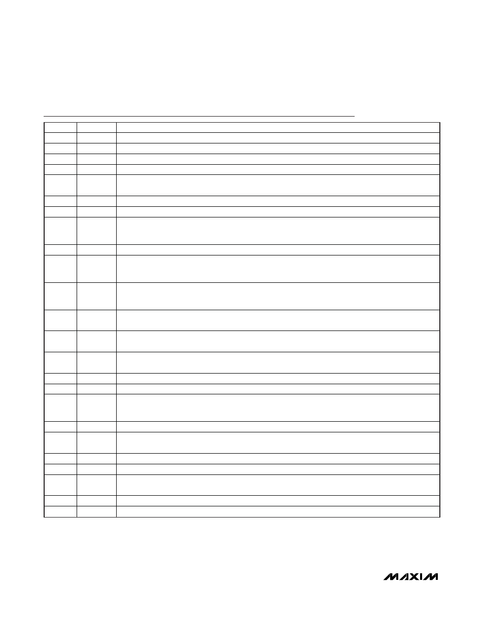
Pin Description
PIN
NAME
FUNCTION
1
POS
Operational Amplifier Noninverting Input
2
NEG
Operational Amplifier Inverting Input
3 OUT
Operational
Amplifier
Output
4
BGND
Analog Ground for Operational Amplifier and Charge Pump. Connect to AGND underneath the IC.
5 SUP
Operational Amplifier and Charge-Pump Supply Input. Connect this pin to the output of the boost
regulator (AVDD) and bypass to BGND with a minimum1μF capacitor.
6
DRVP
Positive Charge-Pump Driver Output
7
DRVN
Negative Charge-Pump Driver Output
8 CTL
High-Voltage Switch Control Input. When CTL is high, the switch between GON and SRC is on and the
switch between GON and DRN is off. When CTL is low, the switch between GON and DRN is on and the
switch between GON and SRC is off. CTL is inhibited by VCC UVLO and when DEL is less than 1.25V.
9
RST
Reset Output. RST is an open-drain output.
10 FBP
Positive Charge-Pump Regulator Feedback Input. Connect FBP to the center of a resistive voltage-
divider between the positive charge-pump regulator output and AGND to set the positive charge-pump
regulator output voltage. Place the resistive voltage-divider within 5mm of FBP.
11 FBN
Negative Charge-Pump Regulator Feedback Input. Connect FBN to the center of a resistive voltage-
divider between the negative output and REF to set the negative charge-pump regulator output voltage.
Place the resistive voltage-divider within 5mm of FBN.
12 REF
Reference Output. Connect a 0.22μF capacitor from REF to AGND. All power outputs are disabled until
REF exceeds its UVLO threshold.
13 VCC
Supplies the Internal Reference and Other Internal Circuitry. Connect VCC to the input supply voltage
and bypass VCC to AGND with a minimum 1μF ceramic capacitor.
14 AGND
Analog Ground for Step-Up Regulator and Linear Regulators. Connect to power ground (PGND)
underneath the IC.
15
RSTIN
Reset Input. Connect to the center of a resistor-divider from V
IN
.
16
COMP
Compensation Pin for Error Amplifier. Connect a series RC from COMP to AGND.
17 FB
Step-Up Regulator Feedback Input. Connect FB to the center of a resistive voltage-divider between the
step-up regulator output and AGND to set the regulator’s output voltage. Place the resistive voltage-
divider within 5mm of FB.
18, 19
PGND
Power Ground
20 LX
Step-Up Regulator Switching Node. Connect inductor and catch diode here and minimize trace area for
lowest EMI power ground.
21
DRN
Switch Input. Drain of the internal high-voltage back-to-back p-channel FET connects to COM.
22
COM
Internal High-Voltage MOSFET Switch Common Terminal
23 SRC
Switch Input. Source of the internal high-voltage pFET. Bypass SRC to PGND with a minimum 0.1μF
capacitor close to the pin.
24
DEL
High-Voltage Switch Delay Input. Connect a capacitor from DEL to AGND to set delay.
—
EP
Exposed Pad. Connect to AGND.