Pin description – Rainbow Electronics MAX5097 User Manual
Page 9
MAX5096/MAX5097
40V, 600mA Buck Converters with Low-
Quiescent-Current Linear Regulator Mode
_______________________________________________________________________________________
9
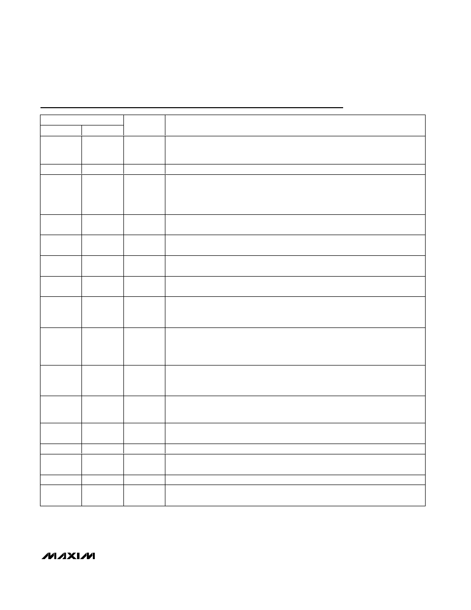
Pin Description
PIN
TQFN
TSSOP
NAME
FUNCTION
1
4
PGND
Power Ground. Return path for p-channel power MOSFET driver. Connect the input
capacitor return, freewheeling diode anode, and output capacitor return terminals to
PGND.
2
5
SGND
Signal Ground. Connect SGND to PGND near the input bypass capacitor return terminal.
3
6
RESET
Open-Drain, Active-Low Reset Output. RESET asserts low when OUT drops below the
reset threshold. When output rises above 92% of the programmed level, RESET
becomes high impedance after the reset timeout period. Connect a pullup resistor from
RESET to the converter output to create a logic output.
4
7
BP
4V Internal Regulator Output. Bypass BP to SGND with a 1µF or greater ceramic
capacitor.
5
9
SYNC
Synchronization Input. Connect SYNC to an external clock for synchronization. Connect
SYNC to SGND when not used.
6
10
SS
Soft-Start Timer Input. Connect an external capacitor from SS to SGND to adjust the soft-
start timeout period (see the Soft-Start (SS) section).
7
11
CT
Reset Timeout Period. Connect a capacitor from CT to SGND to set the reset timeout
period (see the Power-On Reset Output RESET section).
8
12
COMP
Buck Converter (Buck Mode) Control Loop Compensation. See the Compensation
Network section for compensation network design. LDO mode does not need external
compensation.
9
13
LDO/BUCK
LDO Mode/Buck Mode Select. Drive LDO/BUCK low to select the Buck Mode. The Buck
Mode activates after 32 internal/external clock cycles. Force the LDO/BUCK high (> 2V),
to select LDO Mode. The Buck Mode stops and LDO Mode is activated with a 100µs
delay.
10
15
ADJ
Regulator Output Feedback Point. Connect ADJ to SGND for a fixed 3.3V
(MAX5096A/MAX5097A) or 5V (MAX5096B/MAX5097B). For adjustable output voltage,
use an external resistive divider to set V
OUT
. V
ADJ
regulating set point is 1.237V.
11
16
OUT
Converter Output. OUT must always be connected to the regulator output. Connect at
least a 22µF low-ESR (equivalent series resistance) capacitor from OUT to PGND for
stable operation.
12
17
EN
Enable Input. EN is internally pulled to ground. Drive EN high to turn on the regulator.
Force EN low or leave unconnected to place the device in shutdown mode.
13, 14
19, 20
LX
Drain Connection of Internal p-Channel High-Side Switch
15, 16
1, 2, 3
IN
Regulator Input. Bypass IN to PGND with a parallel combination of low-ESR ceramic and
aluminum capacitor to handle the input ripple current.
—
8, 14, 18
N. C.
No Connection. Not internally connected.
EP
EP
EP
Exposed Pad. Connect externally to a large ground plane (SGND) for improved heat
dissipation. Do not use EP as an electrical ground connection.