Absolute maximum ratings, Electrical characteristics – Rainbow Electronics MAX5097 User Manual
Page 2
MAX5096/MAX5097
40V, 600mA Buck Converters with Low-
Quiescent-Current Linear Regulator Mode
2
_______________________________________________________________________________________
ABSOLUTE MAXIMUM RATINGS
Stresses beyond those listed under “Absolute Maximum Ratings” may cause permanent damage to the device. These are stress ratings only, and functional
operation of the device at these or any other conditions beyond those indicated in the operational sections of the specifications is not implied. Exposure to
absolute maximum rating conditions for extended periods may affect device reliability.
(All voltages referenced to PGND, unless otherwise noted.)
IN (transient, 1ms) ..................................................-0.3V to +45V
SGND ....................................................................-0.3V to +0.3V
LX....................................................................-1V to (V
IN
+ 0.3V)
LX Current ................................................................................2A
EN ................................................................-0.3V to (V
IN
+ 0.3V)
BP, SYNC, LDO/BUCK, RESET to SGND...............-0.3V to +12V
BP, RESET Output Current..................................................25mA
CT, SS, ADJ, COMP to SGND ....................-0.3V to (V
BP
+ 0.3V)
OUT ........................................................................-0.3V to +11V
OUT Short-Circuit Duration ........................................Continuous
Continuous Power Dissipation (T
A
= +70°C)*
16-Pin TQFN (derate 33.3mW/°C above +70°C) ........2666mW
20-Pin TSSOP (derate 21.7mW/°C above +70°C) ......1739mW
Thermal Resistance:
(
θ
JA
, 16-Pin TQFN)* ...................................................30.0°C/W
(
θ
JC
, 16-Pin TQFN).......................................................1.7°C/W
(
θ
JA
, 20-Pin TSSOP)* .................................................46.0°C/W
(
θ
JC
, 20-Pin TSSOP)........................................................2°C/W
Operating Temperature Range .........................-40°C to +125°C
Junction Temperature ......................................................+150°C
Storage Temperature Range .............................-60°C to +150°C
Lead Temperature (soldering, 10s) .................................+300°C
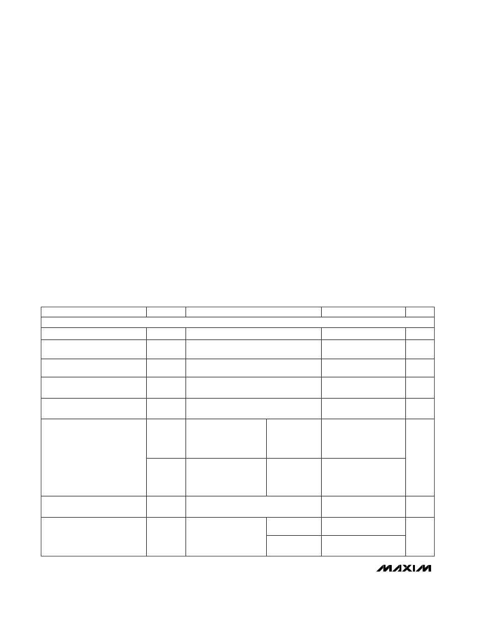
ELECTRICAL CHARACTERISTICS
(V
IN
= +14V, I
OUT
= 1mA, C
IN
= 100µF, C
OUT
= 22µF, L = 22µH, C
BP
= 1µF, V
EN
= +2.4V (Figure 2), SGND = PGND = 0V, T
A
= T
J
=
-40°C to +125°C, unless otherwise noted. Typical values are at T
A
= T
J
= +25°C.) (Note 1)
PARAMETER
SYMBOL
CONDITIONS
MIN
TYP
MAX
UNITS
SYSTEM INPUT
Input Voltage Range (LDO Mode)
V
IN_LDO
LDO/BUCK = high
4
40
V
Input Voltage Range (Buck
Mode)
V
IN_BUCK
LDO/BUCK = low
5
40
V
Internal Input Undervoltage
Lockout
V
UVLO
V
BP
rising
3.5
3.65
3.9
V
Internal Input Undervoltage
Lockout Hysteresis
V
UVLO_HYS
V
BP
falling
0.185
V
BP (Internal Regulator) Output
Voltage
V
BP
V
IN
= +4.5V, I
BP
= 100µA
3.75
4
4.20
V
I
Q
LDO/BUCK = high,
measured at input supply
return, V
OUT
= 5V,
I
OUT
= 100µA
T
A
= -40°C to
+125°C
41
70
Quiescent Supply Current
(LDO Mode)
I
Q
LDO/BUCK = high,
measured at input supply
return, V
OUT
= 5V,
I
OUT
= 100mA
T
A
= -40°C to
+125°C
44
100
µA
Buck Converter No-Load Supply
Current
I
Q_BUCK
V
IN
= 14V, V
OUT
= 5V, I
OUT
= 0
680
µA
T
A
= -40°C to
+125°C
6
19
Shutdown Supply Current
I
SHDN
V
EN
= 0V, measured
from EN
T
A
= -40°C to
+85°C
6
12
µA
*As per JEDEC 51 Standard—Multilayer Board.