Electrical characteristics, Absolute maximum ratings – Rainbow Electronics MAX98500 User Manual
Page 2
2 ______________________________________________________________________________________
MAX98500
Boosted 2.2W Class D Amplifier
with Automatic Level Control
Stresses beyond those listed under “Absolute Maximum Ratings” may cause permanent damage to the device. These are stress ratings only, and functional
operation of the device at these or any other conditions beyond those indicated in the operational sections of the specifications is not implied. Exposure to absolute
maximum rating conditions for extended periods may affect device reliability.
V
BAT
to AGND .........................................................-0.3V to +6V
V
CCOUT
to BSTPGND, AGND .................................-0.3V to +6V
PVDD to SPKPGND .................................................-0.3V to +6V
BSTPGND, SPKPGND to AGND ......................... -0.3V to +0.3V
GAIN to AGND ........................................ -0.3V to (V
BAT
+ 0.3V)
SDBST, SDSPK to AGND ...................................... -0.3V to V
BAT
All Other Pins (excluding LX) to AGND ..................-0.3V to +6V
Current Into/Out of LX, V
CCOUT
, BSTPGND ..................... Q3.9A
Continuous Current Into/Out of SPK_, PVDD,
SPKPGND .................................................................. Q800mA
Continuous Input Current (all other pins) ........................ Q20mA
Duration of Short Circuit Between V
CCOUT
and BSTPGND ...................................................... Continuous
Duration of SPK_ Short Circuit to PVDD or
SPKPGND ..............................................................Continuous
Duration of Short Circuit Between SPKP
and SPKN ..............................................................Continuous
Continuous Power Dissipation, Multilayer Board (T
A
= +70NC)
WLP (derate 20.4mW/NC above +70NC)........................1.33W
θ
JA
(Note 1).................................................................49NC/W
Junction Temperature .....................................................+150NC
Operating Temperature Range .......................... -40NC to +85NC
Storage Temperature Range ............................ -65NC to +150NC
Soldering Temperature (reflow) ......................................+260NC
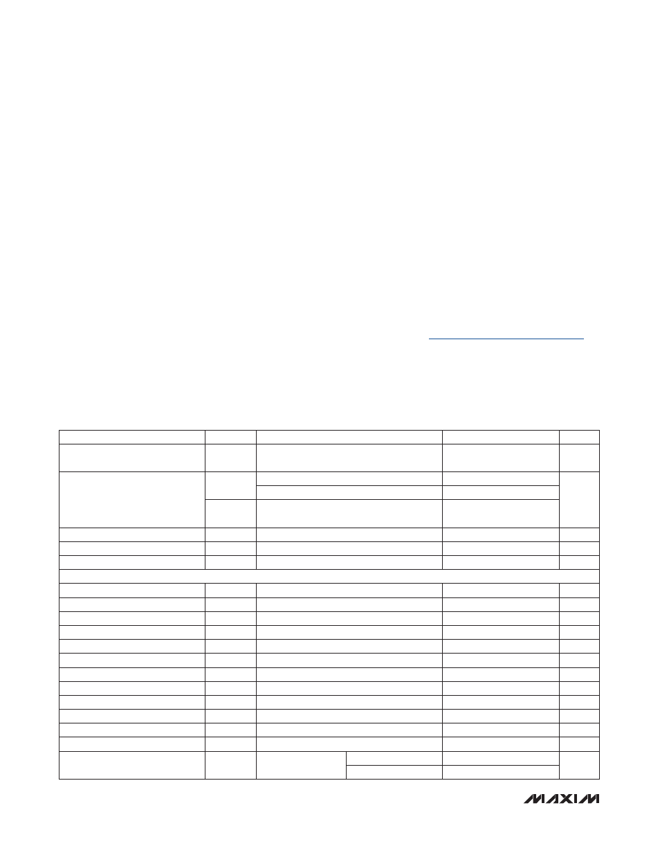
ELECTRICAL CHARACTERISTICS
(V
BAT
= 3.6V, R
L
= J between SPKP and SPKN, A
V
= +6dB, C
IN
= 1FF, 20Hz to 22kHz AC measurement bandwidth, T
A
= T
MIN
to
T
MAX
, unless otherwise noted. Typical values are at T
A
= +25NC.) (Note 2)
ABSOLUTE MAXIMUM RATINGS
Note 1: Package thermal resistances were obtained using the method described in JEDEC specification JESD51-7, using a four-
layer board. For detailed information on package thermal considerations, refer to
www.maxim-ic.com/thermal-tutorial
.
PARAMETER
SYMBOL
CONDITIONS
MIN
TYP
MAX
UNITS
Power-Supply Rejection Ratio
(Note 3)
PSRR
T
A
= +25NC, V
BAT
= 2.5V to 5.5V
95
dB
Quiescent Current
I
VBAT
T
A
= +25NC, SDSPK = SDBST = V
BAT
3.05
mA
T
A
= +25NC, V
SDSPK
= 0V, SDBST = V
BAT
0.09
0.15
I
PVDD
T
A
= +25NC, PVDD = 5.55V, SDSPK =
SDBST = V
BAT
1.7
2.7
Combined Efficiency
E
P
OUT
= 1.7W, f = 1kHz, Z
SPK
= 8I + 68FH
87
%
Shutdown Current
I
SHDN
V
SDSPK
= V
SDBST
= 0V, T
A
= +25NC
0.04
1.5
F
A
Turn-On Time
t
ON
Time from power-on to full operation
10
12
ms
BOOST CONVERTER
Battery Supply Voltage Range
V
BAT
2.5
5.5
V
Soft-Start Interval
t
ON
5.6
ms
Undervoltage Lockout
UVLO
V
BAT
falling
2.1
2.2
2.3
V
Boost Converter Output Voltage
V
VCCOUT
I
LOAD
= 0mA
5.45
5.5
5.65
V
Output Current Limit
I
MAX
V
BAT
R = 3.6V
1.5
A
Input Current Limit
I
LIMIT
Startup, V
CCOUT
= 0V
0.3
0.5
A
nMOS Current Limit
I
LX,MAX
3.3
A
pMOS Turn-Off Current Limit
10
mA
Switching Frequency
f
S
1.8
2.0
2.2
MHz
Efficiency
E
0.1A P I
OUT
P 0.75A
93
%
Startup Short-Circuit Time
Converter latch off
50
ms
Thermal Shutdown
165
N
C
LX Leakage Current
V
LX
= 0V or 5.5V,
V
CCOUT
= 5.5V
T
A
= +25NC
-1.0
+0.1
+1.0
F
A
-40NC P T
A
P +85NC
0.1