Typical application circuit, Supply bypassing, layout, and grounding, Wlp applications information – Rainbow Electronics MAX98500 User Manual
Page 13
______________________________________________________________________________________ 13
MAX98500
Boosted 2.2W Class D Amplifier
with Automatic Level Control
Supply Bypassing, Layout, and Grounding
Proper layout and grounding are essential for optimum
performance. Use a large continuous ground plane on
a dedicated layer of the PCB to minimize loop areas.
Connect AGND and BSTPGND/SPKPGND directly to the
ground plane using the shortest traces length possible.
Proper grounding improves audio performance, and
prevents any digital noise from coupling into the analog
audio signals.
Bypass V
BAT
with a 10FF capacitor and a system
bulk capacitance of 22FF or larger. Bypass PVDD to
SPKPGND with a 0.1FF capacitor and with as minimal a
loop area as possible. Connect SPKP and SPKN to the
speaker using the shortest and widest traces possible.
Reducing trace length minimizes radiated EMI. Route
SPKP/SPKN as a differential pair on the PCB to minimize
loop area, thereby, the inductance of the circuit. If filter
components are used on the speaker outputs, be sure
to locate them as close as possible to the MAX98500 to
ensure maximum effectiveness. Minimize the trace length
from any ground-tied passive components to SPKPGND
to further minimize radiated EMI.
An evaluation kit (MAX98500 Evaluation Kit) is available
to provide an example layout for the MAX98500.
WLP Applications Information
For the latest application details on WLP construction,
dimensions, tape carrier information, PCB techniques,
bump-pad layout, and recommended reflow tempera-
ture profile, as well as the latest information on reliability
testing results, refer to the Application Note 1891: Wafer-
Level Packaging (WLP) and Its Applications on Maxim’s
website at www.maxim-ic.com/ucsp. See Figure 4 for the
recommended PCB footprint for the MAX98500.
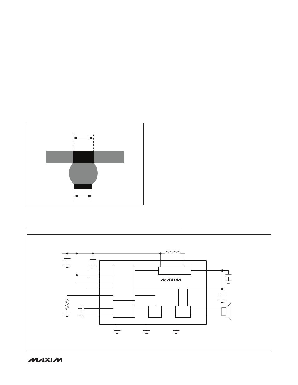
Figure 4. Recommended PCB Footprint
Typical Application Circuit
0.25mm
0.22mm
CONTROL
DIFFERENTIAL
INPUT
BOOST CONVERTER
GAIN
OUTPUT
STAGE
BATTERY
SPKP
SPKN
PVDD
8I
V
CCOUT
LX
V
BAT
22µF*
27.4kI
1%
C
IN
1µF
C
IN
1µF
*SYSTEM LEVEL REQUIREMENT
AGND
SPKPGND
BSTPGND
C4
A4
D1, C2
D3
RKNEE B3
GAIN B2
SDSPK C3
SDBST D4
B4
A3
A2
A1
B1
C1
C
VBAT
10µF
0805
10%
2.2µH
20%
INP D2
INN
MAX98500
C
VCCOUT
22µF
0805
10%
0.1µF
10%