Max6652, Table 2. temperature data format, Table 3. voltage data format – Rainbow Electronics MAX6652 User Manual
Page 6
MAX6652
Writing a 1 to bit 0 of the configuration register starts
the monitoring function. The device will perform a
sequential sampling of all the inputs, starting with the
internal temperature sensor and continuing with 2.5V
IN
,
12V
IN
, 3.3V
IN
, and V
CC
. If the master terminates the
conversion, the sequential sampling will not stop until
the sampling cycle is completed and the results are
stored. When it starts again, it will always start with the
temperature measurement.
An interrupt signal is generated when a temperature
measurement goes above the hot limit or when a volt-
age measurement is either above the high limit or
below the low limit. This will cause the open-drain out-
put (
ALERT) to go to the active-low state and set each
corresponding interrupt status bit (bits 0 through 4) to 1
(Table 5). The interrupt will be cleared by reading the
interrupt status register, except for temperature inter-
rupts generated in comparator mode. Reading the
interrupt status register also clears the register itself,
except for temperature interrupt bits set in comparator
mode.
Unless the fault is removed, the
ALERT output will only
remain cleared until the end of the next conversion
cycle where it will again be asserted. The
ALERT output
can also be masked by writing to the appropriate bits in
the interrupt mask register (Table 6) or by setting bit 1
of the configuration register (Table 4) to 0.
ADC and Multiplexer
The ADC integrates over a 66ms period, an integral
multiple of the line period with excellent noise rejection.
The internal oscillator is trimmed to produce a 66ms
conversion time for temperature and 33ms for each
voltage. This is equivalent to 4 and 2 cycles of 60Hz,
respectively, and provides protection against noise
pickup from the main supply. The internal oscillation
frequency can be changed to provide the same protec-
tion against 50Hz by setting bit 7 in the configuration
register to 1 (Table 4). The multiplexer automatically
sequences through the inputs, measuring voltages, and
temperature.
Temperature Sensor and System Monitor
in a 10-Pin µMAX
6
_______________________________________________________________________________________
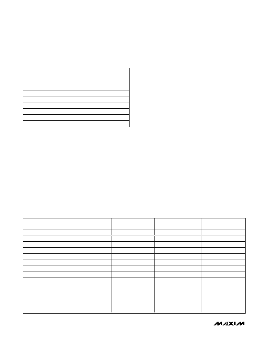
TEMPERATURE
(°C)
DIGITAL
OUTPUT
(BINARY)
DIGITAL
OUTPUT
(HEX)
+125
0111 1101
7D
+25
0001 1001
19
+1
0000 0001
01
0
0000 0000
00
-1
1111 1111
FF
-25
1110 0111
E7
-40
1101 1000
D8
Table 2. Temperature Data Format
ADC OUTPUT
CODE
INPUT VOLTAGE AT
12V
IN
INPUT VOLTAGE AT
2.5V
IN
INPUT VOLTAGE AT
3.3V
IN
V
CC
LSB weight
62mV (12V/192)
13mV (2.5V/192)
17.2mV (3.3V/192)
26mV (5.0V/192)
0
< 62mV
< 13mV
< 17.2mV
—
1
62mV - 125mV
13mV - 26mV
17.2mV - 34.4mV
—
2
125mV - 187mV
26mV - 39mV
34.4mV - 51.6mV
—
—
—
—
—
—
64 (1/4 scale)
4.000V - 4.063V
833mV - 846mV
1.100V - 1.117V
—
—
—
—
—
—
128 (1/2 scale)
8.000V - 8.063V
1.667V - 1.680V
2.200V - 2.217V
3.330V - 3.560V
—
—
—
—
—
192 (3/4 scale)
12.000V - 12.063V
2.500V - 2.513V
3.300V - 3.317V
5.000V - 5.026V
—
—
—
—
—
253
15.813V - 15.875V
3.294V - 3.307V
4.348V - 4.366V
6.566V - 6.615V
254
15.875V - 15.938V
3.572V - 3.586V
4.366V - 4.383V
6.615V - 6.640V
255
> 15.938
> 3.586
> 4.383
> 6.640
Table 3. Voltage Data Format