Detailed description, Table 1. register map – Rainbow Electronics MAX6652 User Manual
Page 5
Detailed Description
The MAX6652 is a voltage and temperature monitor
designed to communicate through an I
2
C-compatible/
SMBus interface with an external microcontroller (µC).
A µC with no built-in I
2
C-compatible or SMBus capabili-
ties can generate SMBus serial commands by “bit-
banging” general-purpose input-output (GPIO) pins.
The MAX6652 can monitor external supply voltages of typi-
cally 2.5V, 3.3V, and 12V, as well as its own supply voltage
and temperature. This makes it ideal for supervisor and
thermal management applications in telecommunications,
desktop and notebook computers, workstations, and net-
working equipment. All inputs are converted to an 8-bit
code using an ADC with an oversampling ratio of 8 to
improve noise rejection. The oversampling ratio can be
reduced by a factor of 4, with a corresponding reduc-
tion in the monitoring cycle time, by setting bit 5 of the
configuration register to 1. Each input voltage is scaled
down by an on-chip resistive divider so that its output,
at the nominal input voltage, is 3/4 of the ADC’s full-
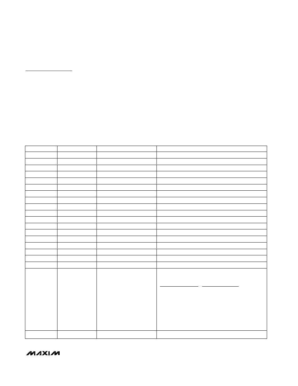
scale range, or a decimal count of 192 (Table 3). Table
1 is the register map and Table 2 is the temperature
data format.
MAX6652
Temperature Sensor and System Monitor
in a 10-Pin µMAX
_______________________________________________________________________________________
5
ADDRESS
READ/WRITE
POWER-ON DEFAULT
DESCRIPTION
20h
R
—
Data register for 2.5 V
IN
measurement
21h
R
—
Data register for 12V
IN
measurement
22h
R
—
Data register for 3.3V
IN
measurement
23h
R
—
Data register for V
CC
measurement
27h
R
—
Data register for temperature measurement
2Bh
R/W
1101 0011 (1.1
✕
2.5V)
High limit for 2.5V
IN
2Ch
R/W
1010 1101 (0.9
✕
2.5V)
Low limit for 2.5V
IN
2Dh
R/W
1101 0011 (1.1
✕
12V)
High limit for 12V
IN
2Eh
R/W
1010 1101 (0.9
✕
12V)
Low limit for 12V
IN
2Fh
R/W
1101 0011 (1.1
✕
3.3V)
High limit for 3.3V
IN
30h
R/W
1010 1101 (0.9
✕
3.3V)
Low limit for 3.3V
IN
31h
R/W
1101 0011 (1.1
✕
5V)
High limit for V
CC
32h
R/W
1010 1101
✕
(0.9
✕
5V)
Low limit for V
CC
39h
R/W
0101 0000
✕
(+80
°C)
Hot temperature limit
3Ah
R/W
0100 0001
✕
(+65
°C)
Hot temperature hysteresis
40h
R/W
0000 1000
Configuration register
41h
R
0000 0000
Interrupt status register
43h
R/W
0000 0000
Interrupt mask register
48h
R/W
0010 1XXY
Device address register. The values of XX are
dependent on the status of the ADD pin.
Power-On Default ADD Connection
0010 100Y To GND
0010 101Y To V
CC
0010 110Y To SDA
0010 111Y To SCL
Y (bit 0) is the SMBus read/write bit. When the 7-
bit chip address is read back from the serial
address register, an 8-bit word will be presented
with a 0 in bit 0 (Y).
4Bh
R/W
0000 0000
Temperature configuration register
Table 1. Register Map