Rainbow Electronics MAX9634 User Manual
Page 2
MAX9634
1µA, 4-Bump UCSP/SOT23,
Precision Current-Sense Amplifier
2
_______________________________________________________________________________________
ABSOLUTE MAXIMUM RATINGS
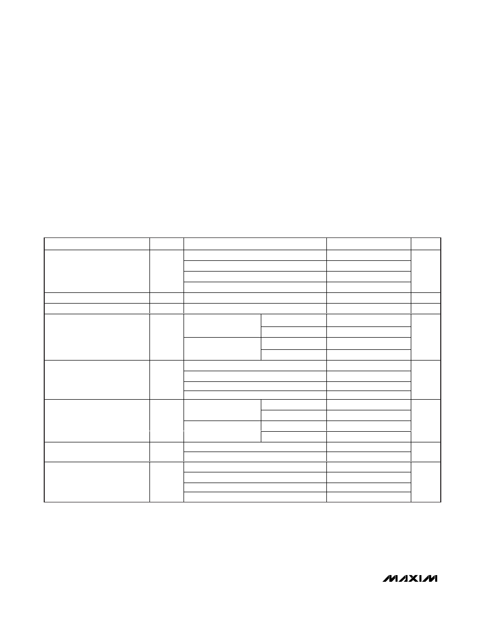
ELECTRICAL CHARACTERISTICS
(V
RS+
= V
RS-
= 3.6V, V
SENSE
= (V
RS+
- V
RS-
) = 0V, T
A
= -40°C to +85°C, unless otherwise noted. Typical values are at T
A
= +25°C.) (Note 1)
Stresses beyond those listed under “Absolute Maximum Ratings” may cause permanent damage to the device. These are stress ratings only, and functional
operation of the device at these or any other conditions beyond those indicated in the operational sections of the specifications is not implied. Exposure to
absolute maximum rating conditions for extended periods may affect device reliability.
PARAMETER
SYMBOL
CONDITIONS
MIN
TYP
MAX
UNITS
V
RS+
= 5V, T
A
= +25°C
0.5
0.85
V
RS+
= 5V, -40°C < T
A
< +85°C
1.1
V
RS+
= 28V, T
A
= +25°C
1.1
1.8
Supply Current (Note 2)
I
CC
V
RS+
= 28V, -40°C < T
A
< +85°C
2.5
µA
Common-Mode Input Range
V
CM
Guaranteed by CMRR, -40°C < T
A
< +85°C
1.6
28
V
Common-Mode Rejection Ratio
CMRR
1.6V < V
RS+
< 28V, -40°C < T
A
< +85°C
94
130
dB
T
A
= +25°C
100
250
MAX9634T/MAX9634F/
MAX9634H
-40°C < T
A
< +85°C
300
T
A
= +25°C
100
250
Input Offset Voltage (Note 3)
V
OS
MAX9634W
-40°C < T
A
< +85°C
425
µV
MAX9634T
25
MAX9634F
50
MAX9634H
100
Gain
G
MAX9634W
200
V/V
T
A
= +25°C
±0.1
±0.5
MAX9634T/MAX9634F/
MAX9634H
-40°C < T
A
< +85°C
±0.6
T
A
= +25°C
±0.1
±0.7
Gain Error (Note 4)
GE
MAX9634W
-40°C < T
A
< +85°C
±0.8
%
MAX9634T/MAX9634F/MAX9634H
7.0
10
13.2
Output Resistance (Note 5)
R
OUT
MAX9634W
14.0
20
26.4
k
Ω
Gain = 25
1.5
7.5
Gain = 50
3
15
Gain = 100
6
30
OUT Low Voltage
V
OL
Gain = 200
12
85
mV
RS+, RS- to GND....................................................-0.3V to +30V
OUT to GND .............................................................-0.3V to +6V
RS+ to RS- ...........................................................................±30V
Short-Circuit Duration: OUT to GND ..........................Continuous
Continuous Input Current (any pin) ..................................±20mA
Continuous Power Dissipation (T
A
= +70°C)
4-Bump UCSP (derate 3.0mW/°C above +70°C).........238mW
5-Pin SOT23 (derate 3.9mW/°C above +70°C)............312mW
Operating Temperature Range ...........................-40°C to +85°C
Junction Temperature ......................................................+150°C
Storage Temperature Range ............................-65°C to +150°C
Bump Temperature (soldering) Reflow............................+260°C
Lead Temperature (soldering, 10s) .................................+300°C
Soldering Temperature (reflow) .......................................+260°C