Rainbow Electronics MAX5106 User Manual
Page 15
MAX5105/MAX5106
Nonvolatile, Quad, 8-Bit DACs
_______________________________________________________________________________________
15
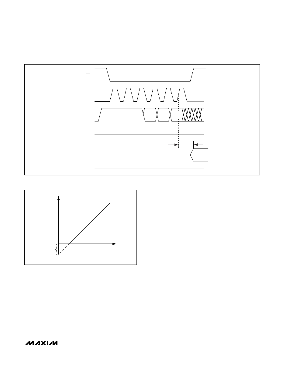
Nonvolatile Load Command
The nonvolatile load command writes the contents of
the selected nonvolatile register to the corresponding
volatile register during the eight clock cycles following
A0. This updates the respective DAC output or
changes the operating state of the device on the rising
edge of CLK corresponding to A0. This command does
not affect the data in the nonvolatile register. Figure 8
shows the nonvolatile load command timing diagram.
RDY/BSY remains high while a volatile register load is
taking place.
Mute/Shutdown Modes
The MAX5105/MAX5106 feature software-controlled
mute and shutdown modes. The shutdown mode places
the DAC outputs in a high-impedance state and reduces
quiescent current consumption to 10µA (max) with all
DACs disabled.
Mute drives the selected DAC output to the correspond-
ing REFL_ voltage. The volatile DAC register retains its
data, and the output returns to its previous state when
mute is removed. The MAX5105 also features an asyn-
chronous MUTE input that mutes all DACs.
The output buffers are individually disabled/muted with
ones in the proper data bits (D7–D0) (Table 1).
When all DACs are muted or shut down, the nonvolatile
store command is ignored. If the mute/shutdown
novolatile register is used to shut down or mute all of
the DACs, use the register write command to change
the operating state of the device. Do this by executing
a register write command that changes the contents of
the mute/shutdown volatile register. Following this, the
nonvolatile store command is again recognized.
Power-On Reset
The power-on reset (POR) controls the initialization of the
MAX5105/MAX5106. During this time, the on-chip oscil-
lator is enabled and used to load the volatile DAC and
mute/shutdown registers with data from the EEPROM.
Figure 8. Nonvolatile Load Command Timing Diagram
DIN
CLK
DOUT
START
C1
C0
A2
A0
A1
HIGH IMPEDANCE
AT V
DD
OUT_
t
COS
(MAX5105 ONLY)
CS
RDY/BSY
Figure 9. Effect of Negative Offset (Single Supply)
O
DAC CODE
NEGATIVE
OFFSET
OUTPUT
VOLTAGE