Functional description – Rainbow Electronics ADC08038 User Manual
Page 14
Functional Description
(Continued)
3 When the start bit has been shifted into the start location
of the MUX register the input channel has been assigned
and a conversion is about to begin An interval of
clock
period (where nothing happens) is automatically inserted
to allow the selected MUX channel to settle The SARS
line goes high at this time to signal that a conversion is
now in progress and the DI line is disabled (it no longer
accepts data)
4 The data out (DO) line now comes out of TRI-STATE and
provides a leading zero for this one clock period of MUX
settling time
5 During the conversion the output of the SAR comparator
indicates whether the analog input is greater than (high)
or less than (low) a series of successive voltages gener-
ated internally from a ratioed capacitor array (first 5 bits)
and a resistor ladder (last 3 bits) After each comparison
the comparator’s output is shipped to the DO line on the
falling edge of CLK This data is the result of the conver-
sion being shifted out (with the MSB first) and can be
read by the processor immediately
6 After 8 clock periods the conversion is completed The
SARS line returns low to indicate this
clock cycle later
7 The stored data in the successive approximation register
is loaded into an internal shift register If the programmer
prefers the data can be provided in an LSB first format
this makes use of the shift enable (SE) control line
On
the ADC08038 the SE line is brought out and if held high
the value of the LSB remains valid on the DO line When
SE is forced low the data is clocked out LSB first On
devices which do not include the SE control line the
data LSB first is automatically shifted out the DO line
after the MSB first data stream The DO line then goes
low and stays low until CS is returned high
The
ADC08031 is an exception in that its data is only output in
MSB first format
8 All internal registers are cleared when the CS line is high
and the t
SELECT
requirement is met See Data Input Tim-
ing under Timing Diagrams If another conversion is de-
sired CS must make a high to low transition followed by
address information
The DI and DO lines can be tied together and controlled
through a bidirectional processor I O bit with one wire
This is possible because the DI input is only ‘‘looked-at’’
during the MUX addressing interval while the DO line is
still in a high impedance state
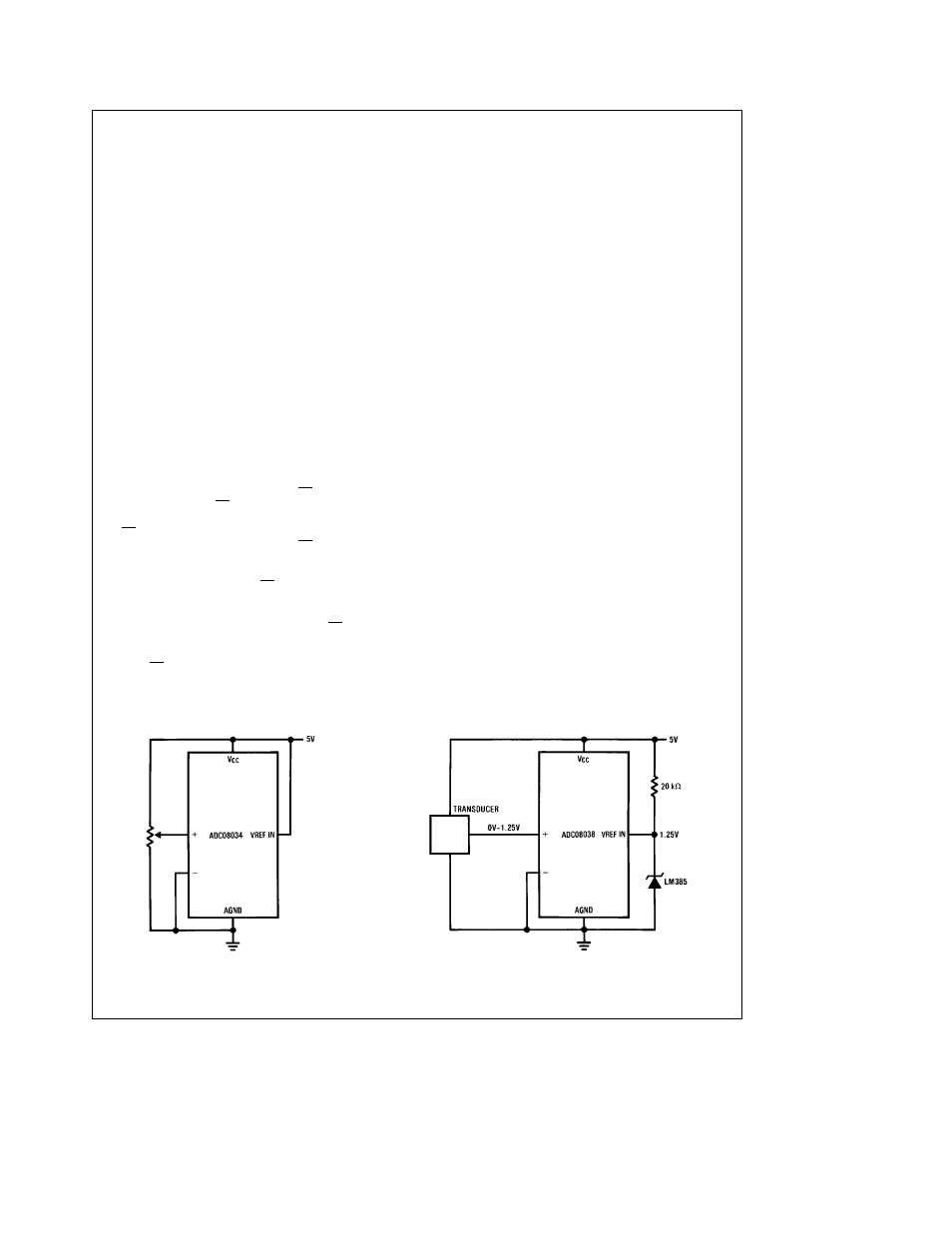
3 0 REFERENCE CONSIDERATIONS
The voltage applied to the reference input on these convert-
ers V
REF
IN defines the voltage span of the analog input
(the difference between V
IN(MAX)
and V
IN(MIN)
over which
the 256 possible output codes apply The devices can be
used either in ratiometric applications or in systems requir-
ing absolute accuracy The reference pin must be connect-
ed to a voltage source capable of driving the reference input
resistance which can be as low as 1 3kX This pin is the top
of a resistor divider string and capacitor array used for the
successive approximation conversion
In a ratiometric system the analog input voltage is propor-
tional to the voltage used for the A D reference This volt-
age is typically the system power supply so the V
REF
IN pin
can be tied to V
CC
(done internally on the ADC08032) This
technique relaxes the stability requirements of the system
reference as the analog input and A D reference move to-
gether maintaining the same output code for a given input
condition
For absolute accuracy where the analog input varies be-
tween very specific voltage limits the reference pin can be
biased with a time and temperature stable voltage source
For the ADC08034 and the ADC08038 a band-gap derived
reference voltage of 2 6V (Note 8) is tied to V
REF
OUT This
can be tied back to V
REF
IN Bypassing V
REF
OUT with a
100mF capacitor is recommended The LM385 and LM336
reference diodes are good low current devices to use with
these converters
The maximum value of the reference is limited to the V
CC
supply voltage The minimum value however can be quite
small (see Typical Performance Characteristics) to allow di-
rect conversions of transducer outputs providing less than a
5V output span Particular care must be taken with regard to
noise pickup circuit layout and system error voltage sourc-
es when operating with a reduced span due to the in-
creased sensitivity of the converter (1 LSB equals V
REF
256)
TL H 10555 – 19
a) Ratiometric
b) Absolute with a Reduced Span
FIGURE 2 Reference Examples
14